Which main drivers will guide your research domain in the coming years?
Arnaud Furnémont: “Today, I see three main drivers pushing for more research on both (active) memory and storage.
First and foremost, there is the persistent demand for more memory per volume and at reduced cost per bit.
This major driver is inextricably linked to the ever-increasing performance of computational systems, which, thanks to advances in both hardware (Moore’s Law) and software (e.g., AI and machine learning) can process ever more data. A second trend is the ‘memory wall’ in data-intensive high-performance computing applications, i.e., the difficulty of accessing the data quickly enough. This drives the research on improving connectivity between logic and memory, for example by using 3D bonding solutions that bring memory dies closer to logic, but also generates needs for high-density embedded memory used as last level of cache. And third, the trend of packing more dies per volume is generating thermal issues – a challenge that is increasingly affecting the memory side of high-performance systems. Think about high-bandwidth memories (HBMs), involving multiple dynamic random access memory (DRAM) dies closely stacked on top of each other.
In the future, I expect other drivers to gain in importance. The evolution towards cryo-CMOS circuits and quantum computing systems may lead to needs of cryo-memory. Also, sustainability will put an ever-increasing mark on memory research, as the global share of wafers that are produced for memory and storage is far larger than for logic. Finally, the evolution towards analog in-memory computing for implementing neural network weights in deep learning applications may open doors to new non-volatile neuromorphic concepts.”
How does industry respond to the quest for larger memory density?
“Throughout the years, industry, in tight collaboration with research institutes such as imec, has explored a range of ‘emerging’ memories – including resistive RAM, magnetic memories (flavors of MRAM), phase change memory (PCM) and ferroelectric memories – for standalone as well as embedded applications. These emerging memories have been investigated to either replace the classical memory and storage solutions (static RAM (SRAM), DRAM and NAND-Flash), or to fill the gap between fast and expensive DRAM, and slow and cheap NAND in traditional computer hierarchies (the so-called storage class memory). Most emerging memories however struggled to get adoption in the market. And this caused memory companies to re-focus on scaling DRAM for the active memory, and NAND-Flash for storage – to meet the classical needs of density.
But there are a few notable exceptions. One is MRAM, which, however not mainstream, is already being used as an alternative option for embedded Flash. On top of that, one of our partners announced to introduce 16nm embedded MRAM to replace SRAM as a last level of cache memories. That could become a game changer for emerging memories.”
Which avenues is imec exploring to remove the primary roadblocks ahead?
“Imec is working on two different fronts.
First, we support our memory partners in extending the roadmaps of classical DRAM and NAND-Flash technologies as far as possible. Second, we investigate new memory concepts that go beyond what exists today.
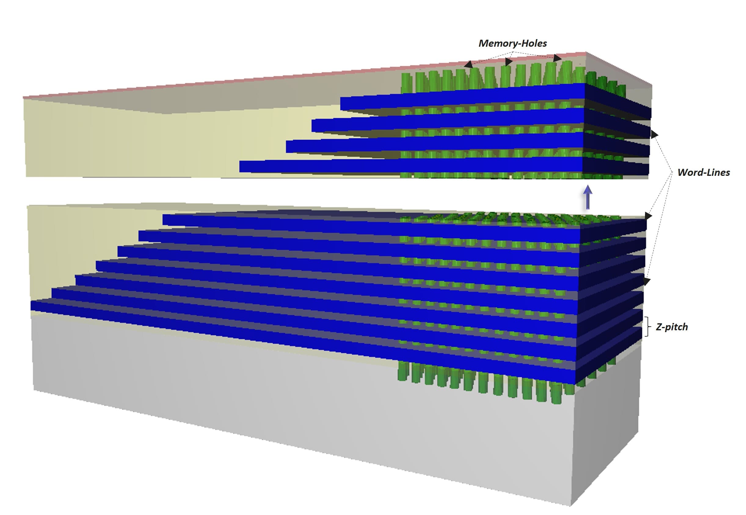
An example is NAND-Flash technology development for storage, which is at the dense, slow, and cheap end of the memory hierarchy. To meet the demand for ever higher bit cell densities, NAND-Flash has moved to the third dimension, with today as many as 176 (word line) layers, and bit cells arranged in a gate-all-around (GAA) architecture. As layer count increases, there is a pressure to shrink the layer thickness (by z-pitch scaling), and to reduce the cell dimensions in xy directions. Imec could demonstrate extremely scaled 3D-NAND-Flash devices with 25nm z-pitch and works on alternative cell architectures (such as the trench cell) to narrow bit cells in the xy direction. In addition, imec expands the storage roadmap into lower latency branches, for which the 3D ferro-electric FET (FeFETs) shows promising characteristics.
In parallel, we look beyond current 3D-NAND-like architectures to identify Tb/mm2 storage options, such as our liquid-based concepts.”
Which breakthrough did your team recently achieve, and what is the relevance for industry?
“At the 2021 IEDM conference, we demonstrated largely improved characteristics of our capacitor-less indium-gallium-zinc-oxide (IGZO)-based DRAM cell, paving the way towards high-density 3D-DRAM as the main computer memory.
Today, industry still uses 1-transistor-1-capacitor (1T1C) cell architectures for enabling planar, scaled DRAM memory arrays, and we believe this classical roadmap can be extended for the next 5 years.
Meanwhile, some of our partners are exploring 3D-DRAM as a path towards higher density standalone DRAM.
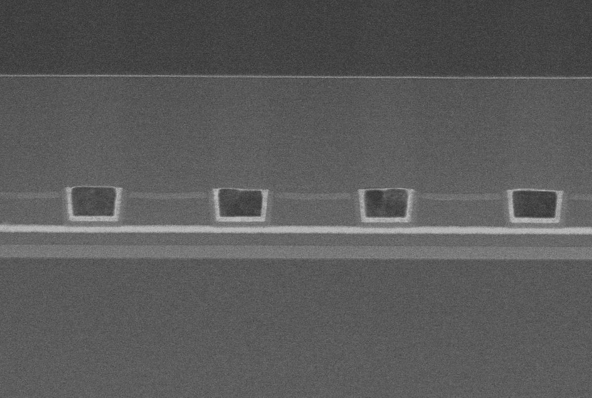
We contribute on the one hand by exploring different ways to fabricate the 3D structure. Our back-end-of-line (BEOL) compatible 2-transistor-0-capacitor (2T0C) IGZO-DRAM cell concept for example allows to move the periphery of the memory cell under the memory array and to stack individual DRAM cells – hence enabling true 3D solutions. On the other hand, we look at channel materials other than IGZO to improve transistor performance and stability.”
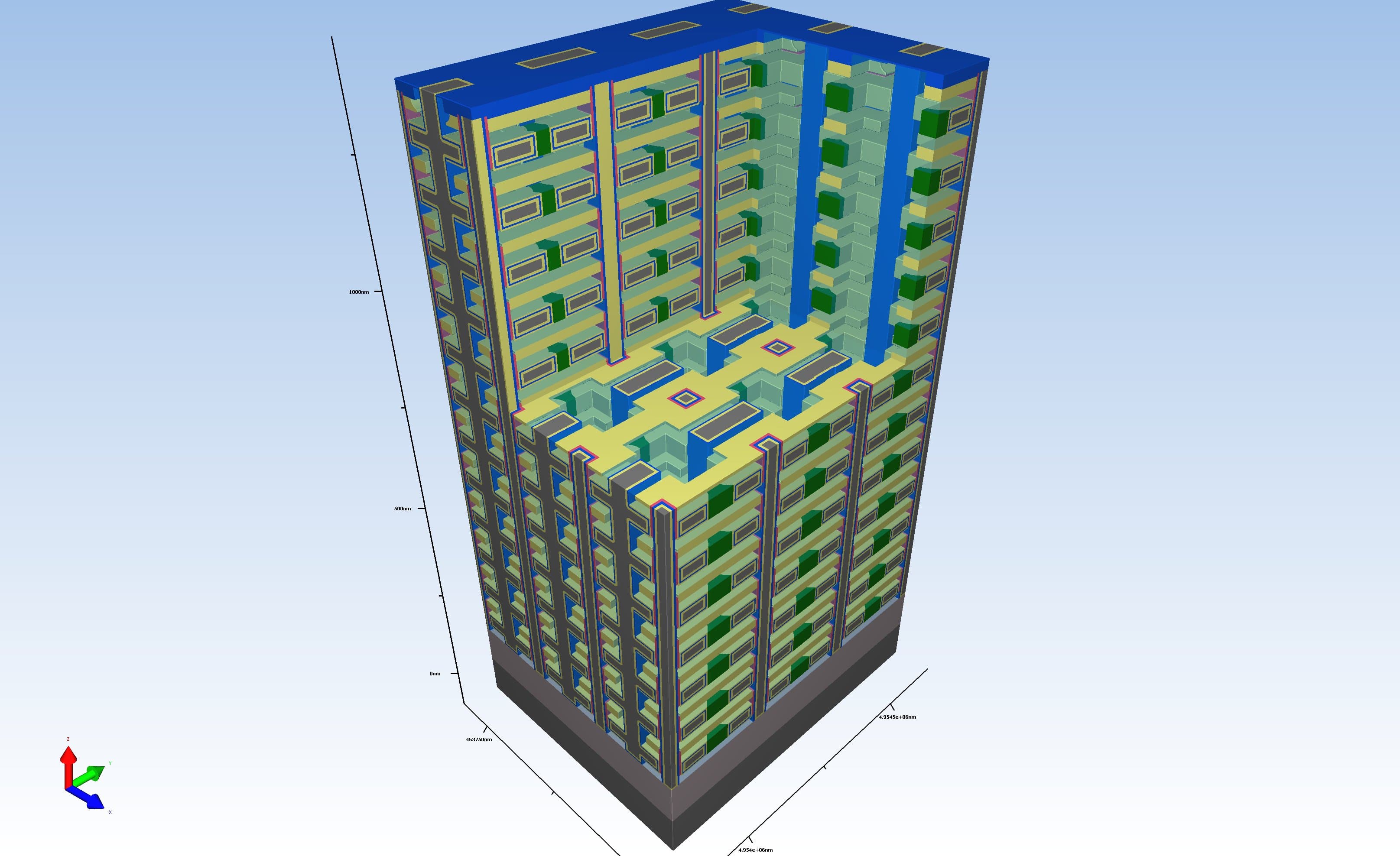
Figure - Example of a potential 3D-DRAM integration based on an alternative semiconductor.
Do you want regular updates on imec’s semiconductor research?
What other new memory concepts are relevant for industry?
“We are investigating three categories of memories that have potential to fit in the DRAM-SRAM space, i.e., low-voltage, dense embedded memories faster than DRAM, able to feed data to logic at very high speed. First, we try to extend the use of IGZO-based 3D-DRAM – introduced above as a high-density standalone memory – towards embedded, logic-compatible applications. Second, we investigate the potential of ferroelectric RAM, a non-volatile 1T1C DRAM-type of memory that implements a ferroelectric material in its capacitor. More specifically, we explore different ferroelectric material systems that can deliver the right properties for DRAM/SRAM-like applications.
And third, we study different flavors of MRAM, including spin-transfer-torque (STT)-MRAM, spin-orbit-torque (VGSOT)-MRAM and fully voltage controlled (VCMA-MRAM) – each trading off speed, power consumption, reliability, and scalability. We develop CMOS-compatible 300mm platforms to bring these technologies to the next level.
Especially promising in view of density is our VGSOT-MRAM device.
This can be arranged in a multi-pillar cell architecture (with multiple magnetic tunnel junction pillars on a common SOT line), whereby one single VCMA top gate selects which one to write. Moreover, VG-SOT enables fast switching in the sub-ns regime, and therefore has all the features to play a role in any category of cache memory.”
There are many stages in developing new (memory) technologies. What stage is the most exciting according to you, and why?
“For me, the most thrilling moments are at the early stages of technology development. A first enjoyable moment is when you feel like having identified the real problem statement. Usually, there is a lot of ‘noise’ about a new field of technology. Take 3D-DRAM as an example. Among the massive amounts of input (papers, patents...), you must be able to filter out what is important and what is the true problem you need to solve – that is a big part of the research. This problem statement then leads to a second great moment, when you start to innovate and solve the problem – exploring, for example, new process flows for 3D-DRAM manufacturing.
In my view, completing these early stages of development is one of imec’s key tasks for industry. This is what our partners are asking us to do. And that requires our researchers to be extremely passionate about technology.”
Want to know more?
- ‘MRAM technologies: from space applications to unified cache memory?’, imec reading room;
- ‘Capacitor-less IGZO-based DRAM cell with excellent retention, endurance and gate length scaling’, imec reading room;
- ‘The role of 3D-NAND-Flash and FeFET in the data storage roadmap’, imec reading room.

After completing his PhD in imec, Arnaud Furnémont joined Intel in Boise and became responsible for 20nm planar Flash reliability, and later on X-Point. In 2013 he came back to imec and served as memory device manager, then memory director with MRAM, SCM, 3D NAND and ferroelectric memory as main focuses. Since 2019, Arnaud expanded his responsibilities to become compute and memory VP for device and integration.
Published on:
8 April 2022

