In search of a memory to fill the DRAM-NAND gap
For several decades, the semiconductor industry has been looking for alternative memory technologies to fill the gap between dynamic random-access memory (DRAM, the compute system’s main memory) and NAND Flash (the system’s storage medium) in traditional high-performance computing system architectures. Such an alternative memory – historically referred to as storage class memory – should outperform DRAM in terms of density and cost and, at the same time, be accessible much faster than NAND Flash. The demand for these memories has recently been fueled by a surge in data-intensive applications like (generative) AI, requiring vast amounts of data to be accessed quickly.
The 1-PCM/1-OTS device: an intermediate solution
Around 2015, the answer came from a new type of non-volatile memory technology called 3D XPointTM, with phase-change memory (PCM) cells arranged at the ‘cross points’ of word and bit lines. PCM memory cells are made of chalcogenide ‘phase-change’ materials (such as germanium antimony telluride (GeSbTe)) sandwiched between two electrodes. The material can quickly and reversibly switch between a high-conductive crystalline phase and a low-conductive amorphous phase – and this resistance contrast is used to store information. Each PCM memory cell is put in series with a selector device, which is needed to address/select the memory cell in the array for program and read operations and to avoid interactions with adjacent cells. While previous versions of PCM used a transistor as a selector device, 3D XPointTM memory makers took a different approach: they used so-called ovonic threshold switching (OTS) devices, made of the same class of material (i.e., chalcogenides) as the PCM bit cell itself.
The technology became available as a commercial product under the brand name Optane from 2017 onwards [1]. While the first generation was introduced at the NAND side of the DRAM-NAND gap, a later generation was pushed towards the DRAM side. This move was facilitated by the simultaneous introduction of the double data rate (DDR) memory interface, providing a much-needed increase in the speed and bandwidth at which data could be transferred between the PCM memory and the memory controller.
Despite the performance improvement, the technology struggled to deliver the required speed, power, and reliability and to retain its place in the memory market. The power issue mainly arises from the high current needed to switch the PCM bit cell. But there were also constraints related to size and cost. One of the major bottlenecks came from the device architecture itself, i.e., the ‘serial’ combination of the bit cell and the OTS selector device.
On first consideration, the 1-PCM/1-OTS outperforms DRAM in terms of cost and area, fostered by the ability to stack the memory array on top of the peripheral circuit. However, these benefits would fade out when one would further increase the density by scaling the bit cell and stacking multiple cross-point layers. The presence of the additional selector device in series with the PCM bit cell would lead to high-aspect-ratio structures and induce expensive lithography and patterning steps in each of the stacked 2D planar layers. Not to mention the increase in complexity when aiming for true 3D devices, where PCM and OTS materials are mounted on a vertical ‘wall’ by conformal deposition – in a 3D-NAND-like fashion. In 2022, the product was withdrawn from the market.
The OTS selector: its role and operation in a cross-point array
When resistive types of memories such as PCM are arranged in a cross-point array, reading and writing of the memory cells ideally takes place only on the selected cell, leaving the rest of the cells unaffected. But in reality, sneak currents run through the unselected cells during memory operation, degrading selectivity and leading to incorrect information retrieval. Selector devices – usually transistors or diodes – are, therefore, connected serially with each resistive memory element. Their role is to address (or select) the memory bit cell for programming/reading and suppress unwanted sneak currents.
Figure 1: Illustration of the role of a selector device (S) in a cross-point architecture with resistive memory elements (R). (Top) Without a selector, sneak currents run through the unselected cells. (Bottom) A selector device serially connected to a resistive memory element prevents the occurrence of unwanted sneak currents.
Do you want regular updates on imec’s semiconductor research?
Ovonic threshold switching (OTS) devices can be a good alternative to transistor-based selectors. OTS devices are named after Stanford Ovshinsky, who discovered reversible electrical switching phenomena in various amorphous chalcogenide materials in the late 1960s. About 50 years later, interest in these materials led to the development of the OTS selector – an OTS material sandwiched between two metal electrodes. When the applied voltage exceeds a specific threshold voltage (Vth), the OTS material experiences a fast drop in resistivity, enabling a high current to flow. This current (Ion) is used to program and read the serially connected memory cell. The other devices in the array are biased in such a way that the voltage is only half of the threshold voltage. At this voltage, the (leakage) current (or Ioff) is extremely low (due to the OTS behavior), and this prevents the undesired programming of adjacent cells.
Figure 2: Typical I-V characteristic of an OTS selector device. At half the threshold voltage, the Ioff current is sufficiently low to prevent interaction with adjacent cells.
OTS selectors have several advantages compared to transistor-based solutions. Unlike transistors, which are three-terminal devices, OTS devices are two-terminal devices. This considerably saves area and enables higher densities. The fabrication of an OTS device is also less expensive. Moreover, OTS materials exhibit a high non-linearity – enabled by the low off current at half the threshold voltage – leading to high selectivity. In addition, they have a large drive current (Ion), can operate at high speed, and have a sufficiently high endurance. And they enable a 3D-compatible solution by stacking 2D planar arrays or enabling true 3D solutions.
The performance and scalability of OTS selectors have improved much over the years, mainly thanks to the past efforts to enable successive generations of the 1-PCM/1-OTS-based Optane memory. In 2015, imec began investigating and developing improved versions of the OTS selector. For example, engineering the material stack for enhanced performance and (thermal) stability, developing new process flows, exploring 3D integration routes, and examining the underlying physical mechanism [2].
Turning point: the observation of a memory effect in OTS devices
While trying to identify the switching mechanism in OTS selectors, researchers at imec observed an interesting phenomenon. When applying a voltage pulse of a certain polarity (so, either a positive or a negative voltage pulse), they observed that the threshold voltage of the OTS device changed noticeably if the previous pulse had the opposite polarity. In other words, the threshold voltage seemed to ‘remember’ the polarity of the previous pulse, even after several hours. This discovery opened doors to the development of ‘OTS-only memories’ that exploit this polarity-induced shift in threshold voltage to store and read information. The beauty of the concept? This single element can act as a memory and a selector in cross-point architectures.
Figure 3: Graph showing the polarity-induced shift in OTS devices. If the read pulse has a different polarity compared to the write pulse, a larger threshold voltage is observed compared to a write-read sequence with the same polarity.
This new memory technology can potentially overcome some of the limitations of 1-PCM/1-OTS memories. Having only one material system for selection and memory makes these devices much easier to fabricate and integrate, benefiting cost and density – especially in 3D configurations. In addition, the current needed to write the device promises to be much lower than the current needed for switching PCM cells, resulting in a more energy-efficient memory technology.
Figure 4: The material system of the OTS-only memory (right) is much simpler than the material system needed to fabricate 1S1R cells (left).
Imec was the first to publicly report this memory effect in SiGeAsTe-based OTS devices in 2021 [3]. After more extensive work, an alternative, Se-based material system led to a practically usable memory window of 1V, defined by the shift in threshold voltage [4]. Meanwhile, other research groups have started to report a similar observation, using a variety of names to describe the memory: OTS-only memory, self-selecting memory, self-rectifying memory, or selector-less memory [5,6,7]. This also led to an increased number of contributions at the recent 2023 IEDM conference, illustrating the growing interest of the semiconductor community in this promising OTS-only memory technology.
Making OTS-only memory technology suitable for CXL memories
A few years ago, the introduction of memory technologies towards the DRAM side of the DRAM-NAND gap was further supported by introducing the compute express link (CXL) interconnect. This open industry standard interconnect offers low-latency and high-bandwidth connections between the memory and the processor in high-performance computing applications. It also resulted in a new name for the class of memories in the DRAM-NAND gap: CXL memories.
While the OTS device had been optimized for selector applications, new requirements were imposed on the technology to be suitable as a CXL memory. The challenge is to find the most optimal tradeoff between endurance, retention, and power consumption. For CXL-type applications, power consumption (mainly determined by the current needed to switch the memory element) and endurance (targeting at least 1012 write/read cycles before failure) are the most critical parameters, while some compromise is allowed on the retention. The retention time determines how long the memory can remain in a well-defined state without being refreshed. For CXL-type applications, a retention of a few hours or days is sufficient. This means the stored information must be refreshed periodically but less frequently than in ‘leaky’ DRAM devices.
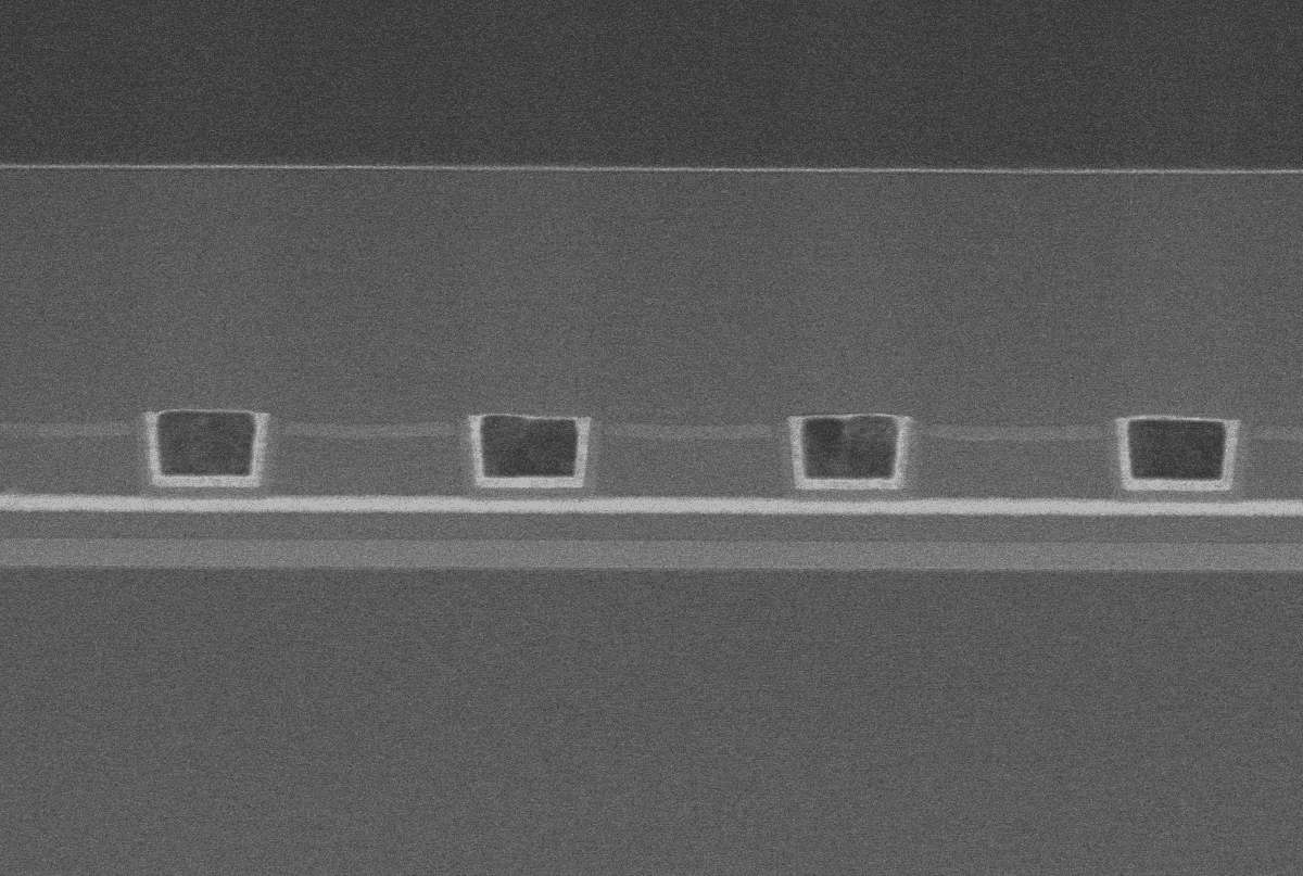
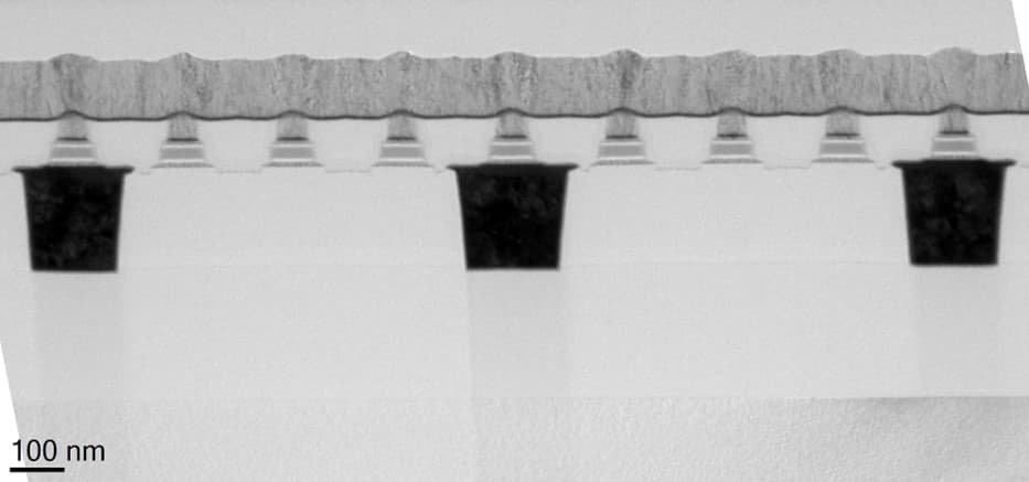
Imec’s state-of-the-art OTS-only memory devices are made of a SiGeAsSe OTS material system sandwiched between carbon-based bottom and top electrodes. The devices, manufactured on a 300mm wafer, are scalable and easy to fabricate and integrate. They exhibit an endurance of >108 cycles, fast read/write operation ensuring low latency (read and write pulses are as short as 10ns), and an ultralow write current <15µA (i.e., <0.6MA/cm2). The latter corresponds to a ~10x energy reduction compared to a typical PCM device. With a half-bias non-linearity NL1/2 ~104, good selectivity is provided, also when operated in memory mode. The polarity-induced voltage shift persists over time, allowing the achievement of a reasonable retention time (>1 month at room temperature). The memory can operate at positive and negative read polarity, showing memory windows of around 1V and 0.5V, respectively.
Figure 5: TEM image of the fabricated SiGeAsSe device with C-based electrodes [4].
Figure 6: (Left) Demonstration of switching at ultralow write current with sufficiently large memory window; (right) memory window for both read polarities as a function of write current [4].
Guidelines for improvement: material research, fundamental understanding, route to 3D integration
The above results highlight the potential of OTS-only memories for CXL applications. Imec has identified critical directions for further research to advance the devices toward industrial uptake.
Material research is needed for several reasons. First, current OTS material systems contain elements such as As and Se that are toxic and not environmentally friendly. Finding alternative eco-friendly material systems that perform as good, or even better, than current OTS materials therefore is a priority.
Second, material and device design optimizations are needed to improve the reliability, i.e., to further enhance the endurance to >1012 and lower the cell-to-cell variability. In addition, the threshold voltage is observed to drift over time, contributing to a cycle-to-cycle variability and impacting the retention time.
Reliability improvement goes hand in hand with a fundamental understanding of the physical mechanism that determines the polarity effect in OTS-only memories. So far, this mechanism is not completely clear. Learning what causes the threshold voltage shift is crucial to explain and predict the observed failures and identify the fundamental tradeoffs that limit device performance.
Finally, imec is exploring routes towards true 3D integration, which will be needed to boost the density of the memory bit cells for next-gen compute system architectures.

Figure 7: Cartoon of an OTS-only memory in a true 3D architecture.
This article was originally published in EDN.
Want to know more?
[1] https://en.wikipedia.org/wiki/3D_XPoint
[2] ‘In pursuit of high-density storage class memory,’ imec reading room, 2017
[3] ‘Polarity-dependent threshold voltage drift in ovonic threshold switches: challenges and opportunities,’ T. Ravsher et al., IEDM 2021
[4] ‘Self-rectifying memory cell based on SiGeAsSe ovonic threshold switch,’ T. Ravsher et al., IEEE Transactions on Electron Devices (T-ED), 2023
[5] ‘Extremely high performance, high density 20nm self-selecting cross-point memory for Compute Express Link,’ S. Hong et al., IEDM 2022
[6] ‘Status and perspectives of chalcogenide-based cross-point memories,’ F. Pellizzer et al., IEDM 2023
[7] ‘Enhanced endurance characteristics in high performance 16nm selector only memory (SOM),’ I.-M. Park et al., IEDM 2023

Gouri Sankar Kar received his Ph.D. in semiconductor device physics from the Indian Institute of Technology, Kharagpur, India, in 2002. From 2002 to 2005, he was a visiting scientist at the Max Planck Institute for Solid State Research, Stuttgart, Germany. In 2006, he joined Infineon/Qimonda in Dresden, Germany, as lead integration engineer and was responsible for vertical transistor development for the DRAM application. In 2009, he joined imec, Leuven, Belgium, where he is currently working as the VP R&D Compute & Memory Device Technologies
Published on:
6 June 2024


