In-memory computing: key to hardware-efficient machine learning
Machine learning, a subset of artificial intelligence, has become integral to our lives. It allows us to learn and reason from data using techniques such as deep neural network algorithms. Machine learning enables data-intensive tasks such as image classification and language modeling, from which many new applications emerge.
There are two phases in the process of machine learning. First is the training phase, where intelligence is developed by storing and labeling information into weights – a computationally intensive operation usually performed in the cloud. During this phase, the machine-learning algorithm is fed with a given dataset. The weights are optimized until the neural network can make predictions with the desired level of accuracy.
In the second phase, referred to as inference, the machine uses the intelligence stored in the first phase to process previously unseen data. The dominant operations for inference are matrix-vector multiplications of a weight matrix and an input vector. For example, when a model has been trained for image classification, the input vector contains the pixels of the unknown images. The weight matrix comprises all the different parameters by which the images can be identified, stored as weights during the training phase. For large and complex problems, this matrix is organized into different layers. The input data are ‘forwarded’ through the neural net to calculate the output: a prediction of what’s contained in the image – a cat, a human, a car, for example.
On the technology side, inputs and weights are usually stored in conventional memories and fetched towards the processing unit to perform the multiplications. For complex problems, a gigantic amount of data thus needs to be moved around, compromising power efficiency and speed, and leaving a large carbon footprint.
However, much of this data traffic can be avoided if (some of) the computational work can be done in the memory itself. When implemented in an energy-efficient way, this in-memory computing reduces the dependence of the inference on the cloud – largely improving latency and energy consumption.
A generic architecture for analog in-memory computing
Unlike traditional memory operations, in-memory computation does not happen at the granularity of a single memory element. Instead, it is a cumulative operation performed on a group of memory devices, exploiting the array-level organization, the peripheral circuitry, and the control logic. The common step is a multiply accumulate operation (MAC), which computes the product of two numbers and adds that product to an accumulator.
While in-memory computation can be performed digitally, this work focuses on its analog implementation, using actual current or charge values. Analog in-memory computing (AiMC) presents several advantages over digital in-memory computing. Provided that multilevel programming is possible, each cell can more easily represent several bits of information (in both weights and inputs), allowing to reduce the number of memory devices. Also, following Kirchoff’s circuit laws, working with charges or currents provides an almost natural way to do the MAC operations.

Figure 1: General concept of multi-vector multiplications for AiMC (as shown at IMW 2023)
In a generic AiMC architecture, the activation signals from the input (or from the previous layer) are first converted to analog signals using digital-to-analog converters (DACs) on the activation lines (figure 1). The analog activation (acti) is then multiplied with the weights (wij) and stored in an array of memory cells. Each cell contributes wij.acti as a current or charge to the summation line. On the summation line, the output is the sum of all the contributions. The output is then converted to digital values. After post-processing, the results are transferred to the next layer or a buffer memory.
In search of a suitable memory technology
Most AiMC-based machine learning systems today rely on conventional static random-access memory (SRAM) technology. But SRAM-based solutions have proven to be expensive, power-hungry, and challenging to scale for larger computational densities. To overcome these issues, the AI community is investigating alternative memory technologies.
At the 2019 ISSCC and IEDM conferences, imec presented a benchmark study of different memory device technologies for energy-efficient inference applications [1,2]. The analysis connected circuit design with technology options and requirements, projecting an energy efficiency of 10,000 tera-operations per second per Watt (TOPS/W), which is beyond the efficiency of the most advanced digital implementations. The researchers identified high cell resistance or low cell current, a low variation, and small cell area as key parameters.
These specifications limit the use of the most popular cell types, including spin-torque-transfer magnetic RAM (STT-MRAM) and resistive RAM (ReRAM). Resistive types of memories store the weights as conductance and encode activation as voltage levels. One of the issues with resistive memories is the IR or voltage drop occurring on both the activation and summation lines, affecting the output. Additionally, a selector device is required for optimized cell access within the array, increasing the cell area and challenges for voltage distribution. Phase change memory (PCM or PCRAM) is limited by similar issues. For spin-orbit torque MRAM (SOT-MRAM), the high current needed to switch the device and the cell’s low on/off ratio is a disadvantage but not necessarily a showstopper.
Of all investigated memory technologies, the imec researchers identified an indium-gallium-zinc-oxide (IGZO)-based 2-transistor 1-capacitor (2T1C) device as the most promising candidate for AiMC. The 2T1C cell, initially proposed for DRAM applications, has two main advantages over SRAM for AiMC applications. First, it enables significantly lower standby power consumption. Second, IGZO transistors can be processed in the chip’s back-end-of-line (BEOL), where they can be stacked on top of the peripheral circuit located in the front-end-of-line (FEOL). This way, no FEOL footprint is required for building the memory array. Further, the IGZO technology also allows stacking multiple cells on top of each other, enabling a denser array.
Engineering IGZO-based 2T1C devices for AiMC applications
At the 2023 International Memory Workshop (IMW), imec researchers addressed the remaining challenges: optimizing the gain cell’s retention time, exploring the possibility of multilevel programming, and demonstrating the MAC operation in an array configuration [3].
Each memory cell within the weight matrix consists of one capacitor and two IGZO transistors. One transistor serves as the write transistor, used to program the weight as a voltage on the (storage node) capacitor, connected to the gate of the second transistor. The second transistor is designed as the read transistor and acts as a current source element, allowing for a non-destructive read. The current through the read transistor depends on both the activation input and the weight stored in the storage node capacitor. This current, hence, naturally represents the output of the multiply operation (wij.acti). Since the readout current is amplified compared to the storage charge flow, 2T1C cells are also referred to as ‘gain cells’.

Figure 2: Schematic of a 2T1C DRAM gain cell.
To be suitable for energy-efficient MAC operations, the three key components of the cell need to meet some target specifications: long retention time, low off currents, and suitable on currents.
The retention time of the gain cell determines how long the cell can retain the programmed weight. The longer the retention time, the less frequently the cell must be refreshed, benefiting power consumption. Also, a long retention time is required for multilevel operation, i.e., the ability to store different voltage levels on the storage node capacitor.
The storage node capacitance is determined by the external capacitor, the gate oxide capacitance of the read transistor, and a parasitic capacitance. The programmed weight can change due to leakage currents. This sets requirements on the leakage currents of the external capacitor and the IGZO transistors – requiring low off currents for the latter.
The read and write transistors mainly differ in the target on current. While a low on current is required for the read transistor to limit IR drop, the on current of the write transistor must be high enough to program the weight in a reasonable write time – i.e., > 1µA/µm.

Figure 3: Stack schematics of the write (left) and read (right) transistors (as shown at IMW 2023).
Amorphous IGZO-based transistors and capacitors have been engineered to meet the different criteria and have been fabricated at a 300 mm wafer scale. The presented solution is CMOS and BEOL compatible, with no FEOL footprint required for fabricating the memory array. The write transistor's high on current and low off current were achieved by adopting a gate last configuration with an oxygen tunnel module and raised source/drain contacts and by using a relatively thick gate dielectric (15 nm). The read transistor has a thinner a-IGZO channel (5 nm) and thinner gate dielectric (5 nm). For the external capacitor, the researchers implemented a 9 nm thick Al2O3-based metal-insulator-metal (MIM) capacitor.
High retention, multilevel programming, and MAC operation: experimental demonstration
As the read and write transistors are engineered differently, they can ideally be integrated on different layers, leveraging the 3D stackability of the IGZO transistors and facilitating denser arrays. To obtain a proof-of-concept for MAC operations, it is, however, sufficient to implement read and write transistors of similar design, i.e., the design of the write transistors.
First, the retention time and off current of a single 2T1C cell were measured. The experiments revealed a retention time as high as 130 s and a median off current as low as 1.5x10⁻¹⁹ A/µm – originating from the wide bandgap of the IGZO channel material.

Figure 4: Evolution of the storage node voltage (VSN) for multiple devices used for estimating retention and off current (as shown at IMW 2023).
To demonstrate multilevel operation, different devices were programmed to different weight levels, and the evolution of the storage node voltages was monitored. Even after 400s, distinct voltage levels could still be observed, showing the ability for single-cell multilevel programming.
Next, the 2T1C gain cells have been implemented in a 2x2 array configuration to verify the MAC operation. The researchers observed increased read current on the summation line when activating two cells on the same activation line (with equally stored weights on the capacitor nodes). This current was almost equal to the sum of currents obtained after activating each cell individually. The results have been extended to 4x2 arrays. In another set of experiments, a change in the summation line’s current was observed when changing the stored weights or the activations. These measurements show that the 2T1C gain cells with IGZO can successfully be used for matrix-vector multiplications in machine-learning applications.

Figure 5: Multilevel MAC operation for a 2x2 array, with storage nodes programmed to different weights (as shown at IMW 2023).
From 2T1C to 2T0C to further reduce cost and area consumption
For the 2T1C cell, a high retention time was achieved by optimizing the transistors and the external capacitor for low off-current and high capacitance, respectively. But earlier work, carried out by imec in the frame of (3D) DRAM applications, proved that a long retention time could also be obtained in a capacitor-less implementation, i.e., in 2T0C gain cells. Thanks to the ultra-low off current in IGZO transistors, long retention is achieved even by only using the gate stack of the read transistor as a storage capacitor. Leaving out the external capacitor has some notable advantages. It lowers the cost and, as the capacitor consumes a considerable area, results in an even smaller footprint. At IEDM 2021, imec presented an IGZO-based 2T0C DRAM cell with >103 s retention time, a consequence of the very low off current of the IGZO transistors [4].
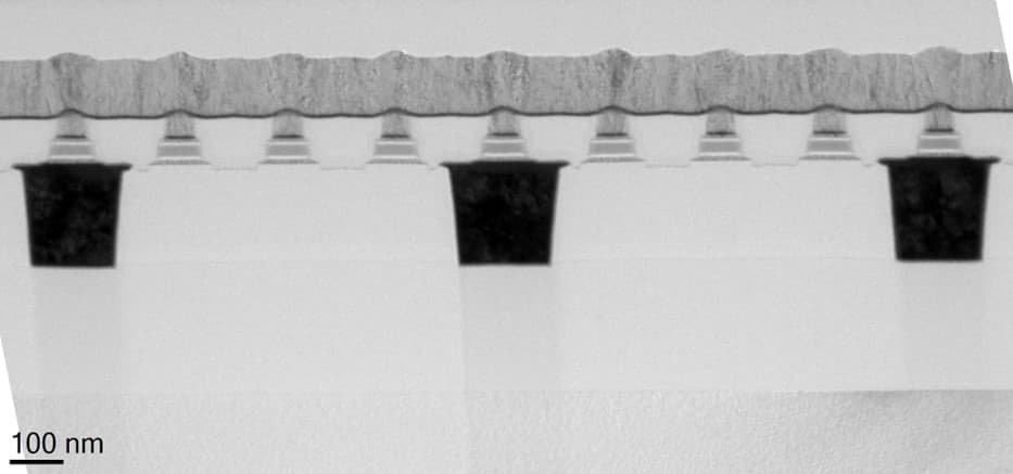
Recently, the imec researchers further improved the retention time of IGZO-based 2T0C devices to > 4.5 hours and achieved an off current < 3x10-21A/µm – the lowest value ever reported for 2T0C devices. Key to these results was using a different technique for patterning the active module of the 2T0C device. The researchers used reactive ion etch (RIE) instead of ion beam etch (IBE). RIE was shown to eliminate metal redeposition induced by IBE, thus suppressing extrinsic leakage paths and extending the retention time. An additional advantage of the RIE technique is the ability to pattern at very small dimensions (sub-100 nm), further reducing area consumption. The results were presented at the VLSI 2023 conference [5].
Thanks to the improved retention, the researchers additionally showed excellent stability of the storage node voltage, indicating favorable analog behavior for machine learning applications. They successfully proved multilevel programming on single-cell 2T0C devices and MAC operation in 2x2 arrays.

Figure 6: (a) 2x2 2T0C array for MAC operation. (b) In the example, cells 1 and 3 are first activated individually. When both are activated, the two currents add up on the SUM line (as shown at VLSI 2023).
Conclusion
IGZO-based 2T1C and 2T0C gain cells show excellent properties for AiMC and can, as such, be used to accomplish the inference phase of machine learning applications. In these applications, they outperform traditional SRAM-based technology regarding energy efficiency and compute density – especially the 2T0C cells excelling in area efficiency. The research has further paved the path to mature this technology for industrial adoption by showing the ability to do multilevel MAC operations.
This article was originally published in Planet Analog.
Want to know more?
[1] ‘Advanced memory, logic and 3D technologies for in-memory computing and machine learning,’ S. Cosemans, ISSCC 2019
[2] ‘Towards 10000TOPS/W DNN inference with analog in-memory computing – a circuit blueprint, device options and requirements,’ S. Cosemans et al., IEDM 2019
[3] ‘Demonstration of multilevel multiply accumulate operations for AiMC using engineered a-IGZO transistors-based 2T1C gain cell arrays,’ S. Subhechha et al., IMW 2023
[4] ‘Tailoring IGZO-TFT architecture for capacitorless DRAM, demonstrating >103s retention, >1011 cycles endurance and Lg scalability down to 14nm,’ A. Belmonte et al., IEDM 2021
[5] ‘Lowest IOFF<3x10-21 A/µm in capacitorless DRAM achieved by reactive ion etch of IGZO-TFT,’ A. Belmonte et al., VLSI 2023
Interested in receiving these articles? Fill in our contact form.

Subhali Subhechha is a senior researcher of memory devices at imec, Belgium. She received her Bachelor’s and Master’s degrees in electrical engineering from Indian Institute of Technology Kanpur. She has been working on different memory devices with imec, Belgium, since 2013. In 2019, she received her Ph.D. in electrical engineering from KU Leuven, Belgium, working on selectorless resistive switching memories. Her current interests are design, modeling, and characterization of oxide semiconductor memories, 3D DRAM, novel memory concepts, and neuromorphic computing. She has served as a member of technical committees in IEDM and IPFA.

Attilio Belmonte is the program manager of active memory at imec, Belgium, where he manages projects related to various memory devices, namely (3D)DRAM, OTS selectors, and FeRAM. He joined imec in 2011 and received his Ph.D. in Physics from KU Leuven, Belgium, in 2015, with a dissertation on novel CBRAM devices. As a researcher, he explored several emerging memory devices, mainly focusing on RRAM, oxide semiconductors, and alternative high-K dielectrics for DRAM. He authored and co-authored more than 85 journal and conference publications.

Gouri Sankar Kar received his Ph.D. in semiconductor device physics from the Indian Institute of Technology, Kharagpur, India, in 2002. From 2002 to 2005, he was a visiting scientist at the Max Planck Institute for Solid State Research, Stuttgart, Germany. In 2006, he joined Infineon/Qimonda in Dresden, Germany, as lead integration engineer and was responsible for vertical transistor development for the DRAM application. In 2009, he joined imec, Leuven, Belgium, where he is currently working as the VP R&D Compute & Memory Device Technologies
Published on:
2 January 2024


