Infrastructure: semiconductor cleanrooms and state-of-the-art labs
Since its creation as an ‘electronics superlab’ in 1984, imec’s infrastructure has been the bedrock of its continued success as the leading global semiconductor R&D center. Today, its three pillars consist of:
- the world’s most advanced 300mm cleanroom for R&D purposes
- our 200mm cleanroom for development on demand, prototyping and manufacturing
- several state-of-the-art labs to support advanced R&D in nano- and digital electronics
- fully-equipped biolabs dedicated to imec’s health and life science R&D activities
Imec’s 300mm cleanroom: world-leading and expanding rapidly
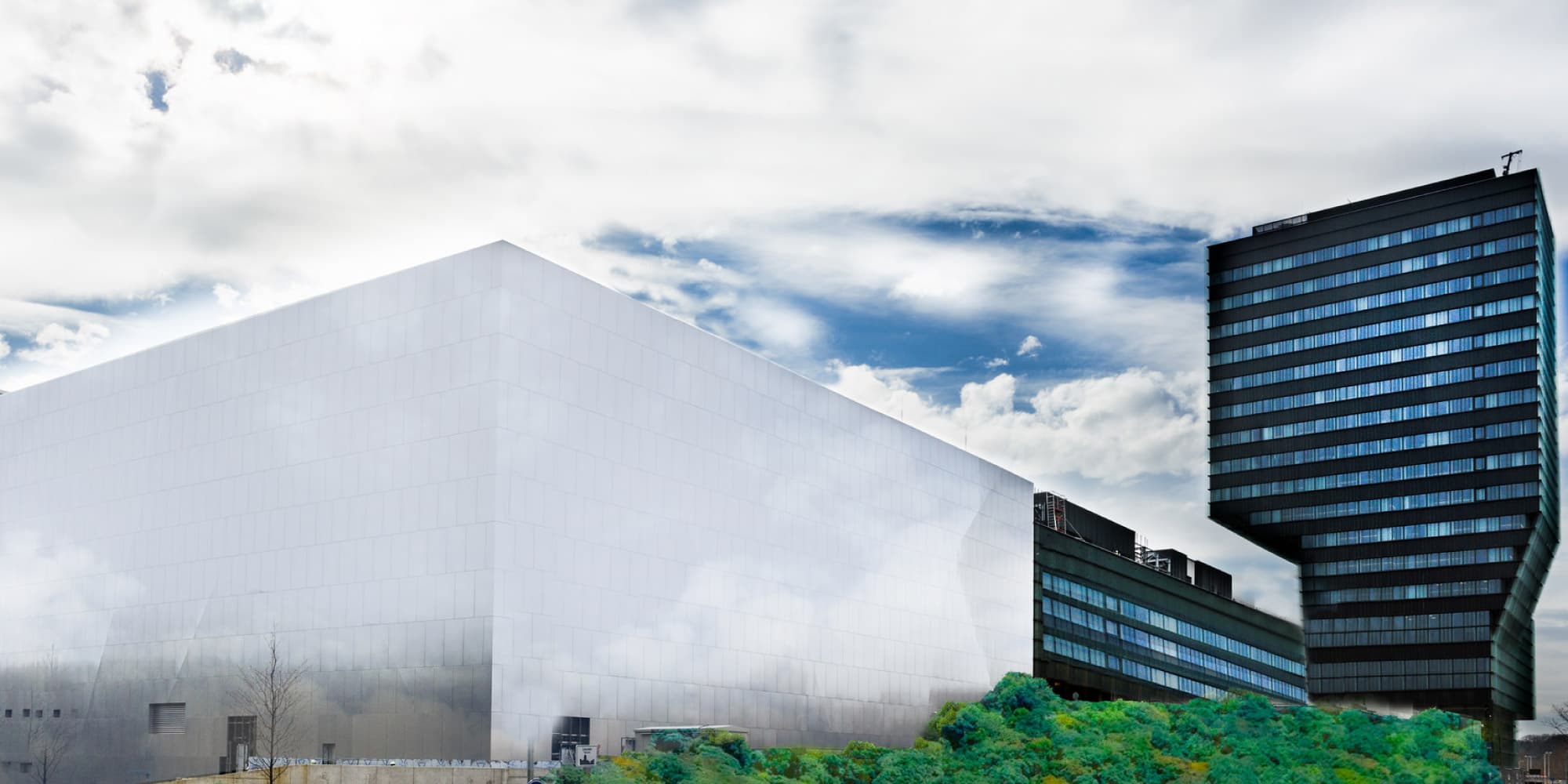
In the beginning of this century, imec launched its pioneering 300mm research program. Since then, the cleanroom in Leuven, Belgium, quickly became a key hub of the global semiconductor ecosystem. Here, the processes that enable the future microchip technology nodes are collaboratively developed and perfected. To this end, the 8,000 m² of cleanroom space is filled with the world’s most advanced industry-relevant equipment – from all leading OEMs including many European suppliers – for lithography, implant, cleaning, metrology, deposition, etc.
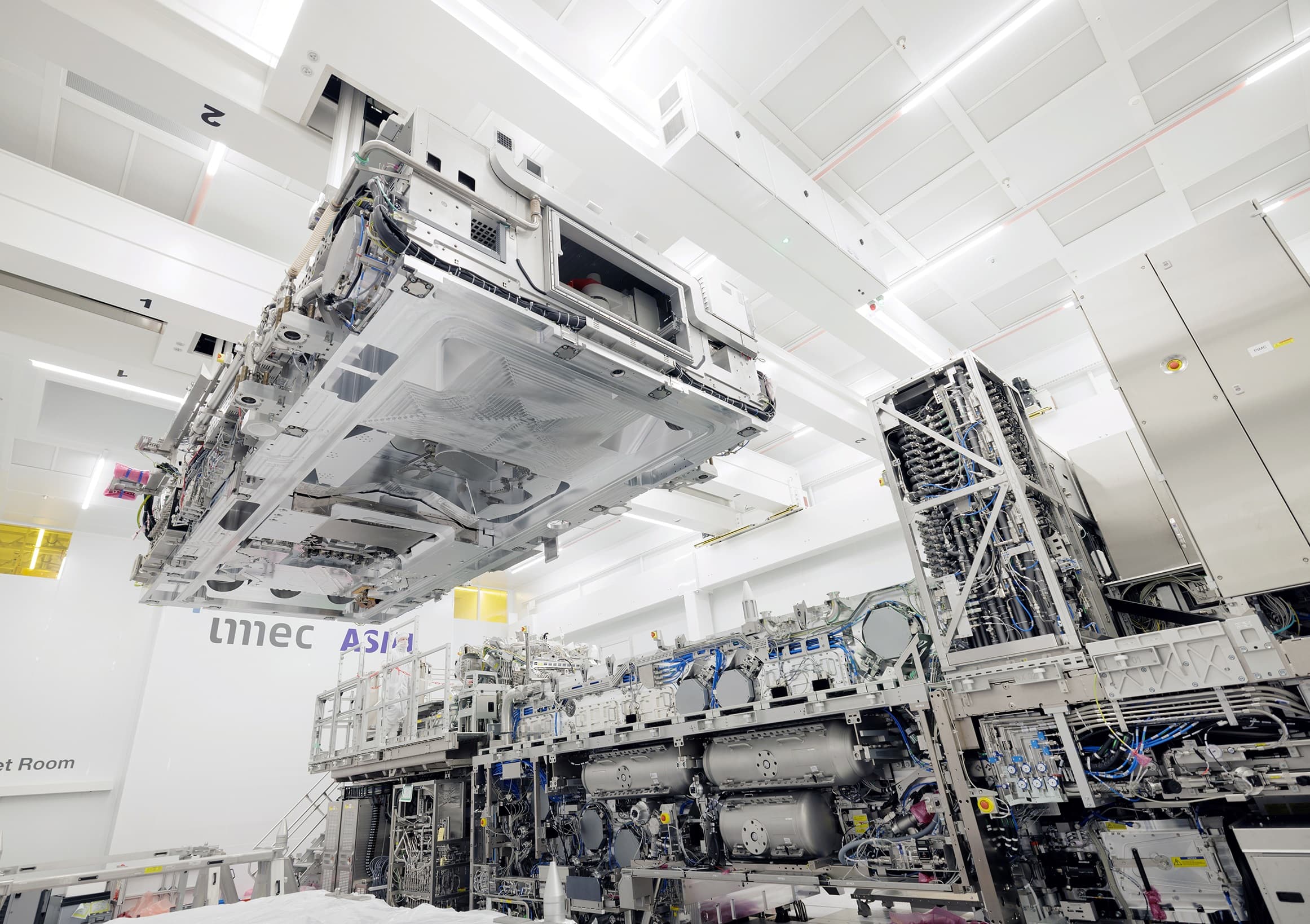
A particularly noteworthy illustration of imec’s key role in advancing the semiconductor roadmap is its collaboration with ASML towards EUV lithography and more recently High NA EUV lithography. Currently, the joint High NA Lithography Lab in Veldhoven, The Netherlands, is where memory and chip manufacturers get access to the high-NA EUV prototype scanner and surrounding tools to prepare this technology for its introduction into major foundries.

Joint High NA Lab of imec and ASML
Thanks to EU Chips Act funding, imec’s 300mm infrastructure will be now extended with a new cleanroom, and dozens of additional advanced tools for processing and metrology. The efficiency of fab operations will also be elevated to new heights through increased tool automation, more connected instruments with central data storage, and automated stocker connections between the cleanrooms on the campus of imec Leuven.
The goal of the resulting NanoIC pilot line is to further accelerate the innovation needed for enabling future compute systems. This is achieved by speeding up the R&D learning cycles and bringing new technologies to a higher level of maturity.
The NanoIC pilot line will focus on 9 technology enablers towards future hpc systems:
Advanced logic
- nanosheet baseline and platformization supporting A14 and A10 nodes
- CFET baseline targeting A7 and beyond nodes
- High NA EUV single-print pathfinding
Novel memory concepts
- SOT-MRAM
- embedded DRAM with 2T0C bit cells
- 3D memory (3D DRAM)
3D integration and optical I/O
- die-to-wafer (D2W) hybrid bonding at 2µm pitch silicon prototyping system
- fine-pitch redistribution layers (RDL)
- III-V laser integrated light sources
These baseline flows will have a technology readiness level of 3-6, much higher than typical research flows. This platformization and its repeatability, variability and defectivity improvements allows:
- IDMs and foundries to test new technologies and performance enhancement options
- equipment and material suppliers to validate tools and process capabilities
- start-ups, design and system companies to perform system pathfinding and prototyping through readily available PDKs
At the same time, advanced R&D into exploratory logic, memory and interconnect technologies, that shapes the long-term roadmaps of our partners remains one of the core purposes of our research infrastructure – and will also benefit from the established platforms.
Imec’s 200mm cleanroom
The 5,200 m² of imec’s 200mm cleanroom, of which 1,750 m² is in class 1, is available for development on demand, prototyping, and manufacturing.
Several mature platforms are available, often with a PDK:
- silicon photonics, co-integrating a wide variety of passive and active components
- silicon nitride photonics, both based on LPCVD and PECVD technology
- MEMS & 3D integration, with advanced integration features such as TSV, direct low-temperature bonding, and micro-bumps assembly
- microfluidics, including monolithic integration with silicon electronics, micro-optics and photonics
- nano-optics, such as filters, polarizers and lenses processed on glass or post-processed on top of device wafers
Furthermore, a wide range devices that require special process steps, such as custom CMOS imagers and GaN-on-Si devices, can be developed in imec’s 200mm cleanroom. And because of the compatibility of these tools with those in major foundries, the manufacturing process can be transferred to high-volume fabrication.
State-of-the-art laboratories
- RF & high power lab
- neuroelectronics lab
- silicon PV Lab
- organic PV Lab
- ExaScience Lab
- ultra-large-scale-integration design methodology lab
- microsystems lab
- ultra-clean processing lab
- lab for material and device characterization
- lab for physico-chemical-analysis
- lab for automatic device and circuit measurement
- organic electronics lab
- packaging and testing equipment lab
- reliability lab
- hyperspectral imaging lab & demo room
- customized imager process line on 130nm CMOS technology
- measurement and testing lab
- GaN lab
- photonics labs
- integrated imagers lab
- material analysis & testing lab at IMO-IMOMEC
- advanced metrology solutions lab
NERF laboratories – Neuro-Electronics Research Flanders
- approximately 1,000 m2 biolab space
- located on the imec campus
- full access to imec facilities: electronic workshop, mechanical workshop, state-of-the-art cleanrooms, biolabs
- full access to the facilities of KU Leuven and VIB
- in close proximity to Science and Engineering Departments of KU Leuven and University Hospital
Biolabs
500m2 of laboratory space is dedicated to imec’s health and life science R&D activities.
Surface and bioassay characterization
- contact angle (CA) measurements
- cyclic voltammetry (CV)
- grazing angle Fourier transform infrared spectroscopy (GA-FTIR)
- quartz crystal microbalance (QCM)
- surface plasmon resonance (SPR)
- confocal laser scanning microscopy (CLSM)
- fluorescence labeling
- nanoparticle characterization
- ultraviolet (UV) spectroscopy
- Qnano® tool
- dynamic light scattering (DLS)
- zeta potential measurements
- thermo-gravimetric analysis (TGA)
- dark field microscopy (DFM)
- dot blot analysis
Biosensor setups
Commercial biosensors
- SPR devices (Biacore2000® and Biacore3000®)
- QCM system
In-house developed biosensors
- optical biosensors (Si ring resonator, localized surface plasmon resonance biosensor)
- nanopore biosensor
- optical hyperthermia biosensor
- magnetic hyperthermia biosensor
DNA research
The imec campus hosts a fully operational laboratory to conduct basic DNA research.
State-of-the-art biological safety level (BSL)-2 laboratory
- optical tweezer setup to manipulate single cells
- cell and tissue culturing facilities
- electrophysiology set-up
- optical microscopy
- patch-clamp confocal microscopy (PCCM)
- fluorescence microscopy
- confocal microscopy for living cells
- live microscopy setup (calcium imaging and membrane integrity testing)
- image post-processing and data analysis
Electrophysiology
- extracellular electrophysiological multi-electrode array (MEA) setup
- 16-channel probe setup
- 4-channel clinical in-vivo recording setup with all recording, stimulation, and signal post-processing equipment
- stereotaxic surgery setup including stereomicroscope
- patch clamp- or MEA-based (commercial and custom imec) recordings, stimulation, and electroporation
- in-vivo recordings and stimulation (commercial and imec custom probes)
Electrochemical characterization
- multichannel multiplexed potentiostat/galvanostat electrochemical measurement system
- cyclic voltammetry techniques for material deposition or characterization
