Why SOT-MRAM can replace SRAM in future cache memories
For many decades, ultrafast and volatile SRAM has been used as embedded cache memory in high-performance compute architectures, where it resides very close to the processor in a multi-level (L1, L2, L3...) hierarchical system. Its role is to store frequently used data and instructions for quick retrieval, with L1 being the fastest of all cache memories. SRAM bit density scaling has been slowing down for some time, and bit cells increasingly suffer from standby power issues.
The spin-orbit torque (SOT) MRAM memory solution has several advantages, such as low standby power consumption, GHz-level switching or write speeds, negligible leakage, practically unlimited endurance, high reliability, and scalability. For these reasons, the industry is increasingly evaluating SOT-MRAM as a promising alternative to SRAM in embedded last-level cache-memory applications.
The basic building block of an SOT-MRAM memory device is a magnetic tunnel junction (MTJ), which consists of a thin dielectric layer (MgO) sandwiched between two ferromagnetic layers (CoFeB-based). One of the ferromagnetic layers has a fixed (or pinned) magnetization, while the other layer has a freely rotating magnetization along the z-axis. The magnetization direction of the ferromagnetic layers can be either perpendicular or parallel to the layers’ plane, referred to as perpendicular MTJs and in-plane MTJs, respectively.
SOT-MRAM memory bit cells are read out by applying a current through the MTJ and measuring the junction’s tunnel magnetoresistance (TMR). The TMR can be high or low, depending on the relative orientation of the magnetizations of the free and fixed layers (i.e., parallel (1) or antiparallel (0)).
Do you want regular updates on imec’s semiconductor research?
Figure 1 – General principle of the MRAM TMR read operation (upper green = fixed layer, lower green = free layer; blue = MgO dielectric layer; i = read current).
The memory cells are written by injecting a spin-polarized current into the MTJ, switching the magnetization of the free layer through spin-orbit interactions. Current injection happens laterally underneath the MTJ, through an adjacent SOT layer (or SOT track) – typically a heavy metal such as tungsten. As such, the read and write paths are de-coupled, ensuring reliable operation. It is in this write operation that SOT-MRAM differs from STT-MRAM, another MRAM flavor where a write current is injected perpendicularly into the MTJ. During the STT-MRAM write operation, a large amount of current tunnels through the MgO barrier.
State-of-the-art SOT-MRAM devices
The memory community has made significant progress in developing SOT-MRAM technology in recent years. Imec also contributed to this progress with groundbreaking improvements. Following an initial public announcement at VLSI 2018, imec reported progressive innovations to address the key challenges on the road to cache applications [1,2].
So far, state-of-the-art SOT-MRAM single devices with switching speeds down to 300ps have been demonstrated on 300mm wafers [3,4]. The adoption of perpendicular MTJ magnetization was considered an important step toward improving the scaling potential.
Progress was also made in enhancing SOT-MRAM’s technology readiness level by removing the need for an external magnetic field during the write operation. Such a field is needed to ensure deterministic magnetization switching. The absence of an external magnetic field leads to unreliable write operations with a write success of 50 percent. From a manufacturing point of view, operating a memory device with an external field is not feasible at the product level. Thus, it is imperative to develop field-free SOT-MRAM device technology. Imec demonstrated a field-free switching approach by incorporating an in-plane magnetic layer as part of the SOT track. The in-plane field induced by this magnetic layer takes over the external magnetic field’s role, enhancing the practical applicability of the technology [3,4].
Solutions have also been proposed to lower the dynamic power consumption associated with the high injection current needed to switch the free layer’s magnetization. At IEDM 2022, imec demonstrated a voltage-gate assisted approach during write operation, lowering the energy barrier for switching [3,4]. The voltage-gate assisted approach also enabled bit cell area reduction, making it attractive for high-density SRAM applications.
The switching energy could be further improved by scaling the dimensions of the SOT track. In conventional SOT-MRAM designs, the area occupied by the underlying SOT track is larger than the actual MTJ pillar footprint to provide sufficient margin for overlay process control. But this results in wasted energy, as part of the injection current flows outside the MTJ area. At IEDM 2023, imec showed that it is possible to scale SOT-MRAM devices to their extreme, with SOT track and MTJ pillar having comparable footprints: a milestone towards large bit cell density [5,6]. For these single devices, a switching energy below 100 femto-Joule per bit and endurance of beyond 1015 program/erase cycles was demonstrated.
What comes next: SOT-MRAM device performance and reliability improvement, and array integration
While key specs such as switching speed and endurance have been achieved, re-designing the material stack brings opportunities to further optimize performance and reliability parameters like retention, BEOL compatibility, robustness against external magnetic influences, and write error rate (WER). WER is a key reliability concern, referring to the probability that the ferromagnetic free layer does not switch when a write current is applied.
In addition, while research efforts mainly focused on device improvement, a crucial step towards industrial adoption is the large-array integration of scaled SOT-MRAM devices. In these array demonstrators, many memory bit cells now connect to the underlying circuitry, which contains the transistors that provide read and write access and bring current and voltages in and out of the bit cells.
Both device improvement and array integration will bring the technology closer to real-world specifications. Addressing all these issues usually involves making trade-offs between different parameters. Recent work at imec, presented at 2024 VLSI and IEDM, focused on improving them as much as possible through integration optimization and materials and device re-design – supported by simulations. This work is summarized below.
At device level: novel free-layer stack leads to more reliable switching of SOT-MRAM devices
At IEDM 2024, imec proposed an innovative composite free layer for the MTJ, leading to more reliable switching of an SOT-MRAM device [7]. The novel free-layer stack is made of a synthetic antiferromagnetic (SAF) structure, i.e., two ferromagnetic layers antiferromagnetically coupled through a Ru layer. This system is then integrated with the conventional CoFeB layers for the TMR readout. The novel stack allows the independent optimization of the TMR (critical for the read operation) and SOT switching operation (providing a path to improve the efficiency of the write operation further).
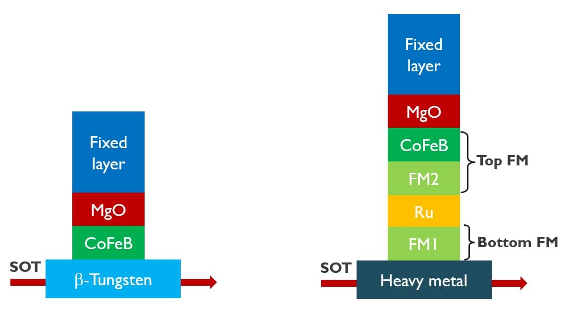
Figure 2 – Schematics of (left) conventional MTJ stack, and (right) MTJ stack with SAF-based free layer (FM1/Ru/FM2). The top free magnetic layer FM2 of the SAF structure is ferromagnetically coupled with CoFeB/MgO for electrical readout of the SAF using TMR (as presented at IEDM 2024 [7]).
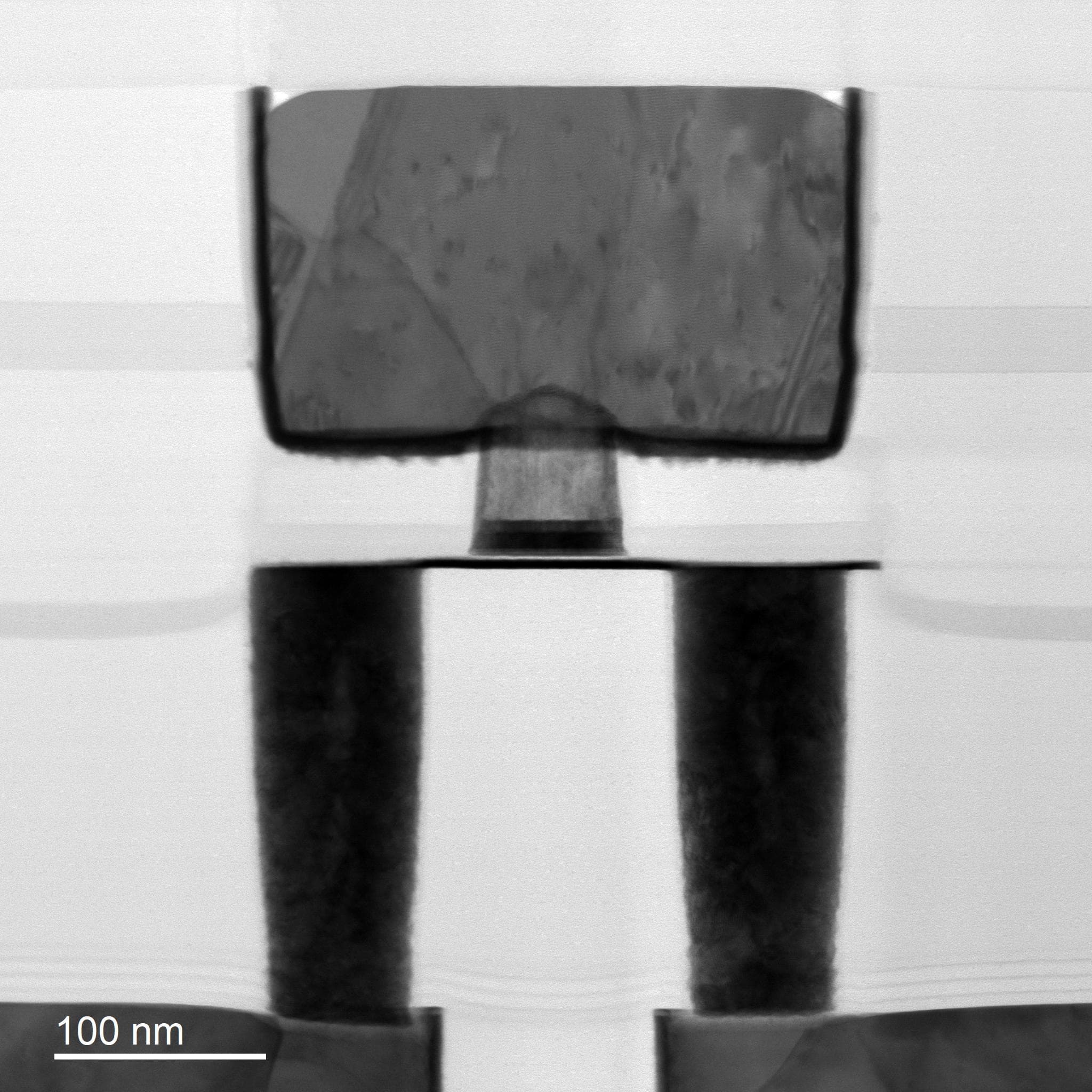
Figure 3 – TEM cross-section image of an SOT-MRAM device with SAF-based free layer (as presented at IEDM 2024 [7]).
SOT-MRAM devices with this composite free layer showed an improved WER, meeting the target spec of 10-6 for the first time. Data retention improved from ∆~50 to ~90 compared to devices with conventional free layers. On the readout side, the TMR could be further enlarged without affecting the SOT switching behavior. In addition, the composite free layer withstands temperatures up to 400°C while maintaining its magnetic properties, making it compatible with BEOL processing. The SAF free layer also makes the SOT-MRAM device less sensitive to external magnetic perturbations.
In this work, imec researchers used micromagnetic simulations to guide material stack design, leading to the most optimal results. The combination of simulations and experiments is crucial for advancing SOT-MRAM technology.
Magnetic immunity of MRAM devices: the role of the external magnetic field orientation
MRAM device operation is fully electrically controlled, but external magnetic fields can easily corrupt the device performance. This reliability issue triggered a broader, worldwide investigation of magnetic immunity. The study aims to better understand the mechanisms at play and guide MRAM design for improved protection. In addition, application-dependent standards are being developed to qualify the MRAM’s robustness against magnetic fields, specifying the field strengths at which stored data are still protected.
At IEDM 2024, imec provided the first experimental evidence that not only the strength but also the orientation of external magnetic fields can negatively impact the active write magnetic immunity of MRAM devices, observed as a deterioration of the WER [8]. The study was conducted on STT-MRAM devices, but the main conclusions are also expected to be valid for SOT-MRAM devices. The experiments involved applying external magnetic fields (between 4 and 40mT) at various angles to perpendicular MTJ stacks and measuring the impact on the WER. A significant reduction of the writing reliability was observed already at fields as low as 10mT under specific external magnetic field angles.
The experiments could successfully be linked to earlier theoretical findings. The insights will help designers in developing MTJ stacks that are less susceptible to angle-dependent WER deterioration in real-world applications.
At array level: successful integration of extremely scaled SOT-MRAM devices
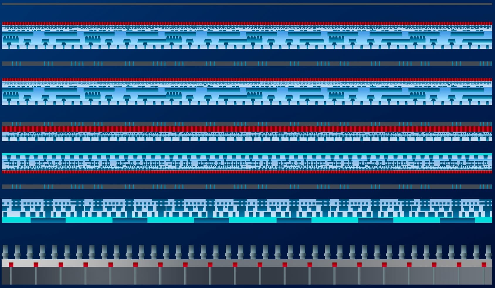
One remaining step is demonstrating the feasibility of integrating the optimized SOT-MRAM devices into large arrays along with the logic circuitry. At VLSI 2024, imec, for the first time, presented a functional array that can serve as a platform for characterizing various SOT-MRAM configurations that have proven to work well at device level. The array is even more versatile, as it can also be used for characterizing STT-MRAMs [9].
Figure 4 – Image of the SOT CMOS array (as presented at VLSI 2024 [9]).
For example, imec has used the array to characterize SOT-MRAM devices that have been scaled to their extreme by reducing the dimensions of the SOT track. As outlined above, these devices work well at the device level, showing improvements in switching energy and endurance [5,6]. The device integration process flow dictates that the SOT tracks are patterned after the MTJ pillars are formed. In extremely scaled devices, where the SOT track width is reduced to the diameter of pillars, the pillars’ sidewalls can easily be exposed and damaged by the successive SOT patterning steps. Imec researchers proposed a novel integration solution to solve that issue. They showed that a double encapsulation of the MTJ pillar, using both SiN and AlOx, could protect the structure during SOT module process steps without affecting critical performance parameters such as the read window at the array level [9].
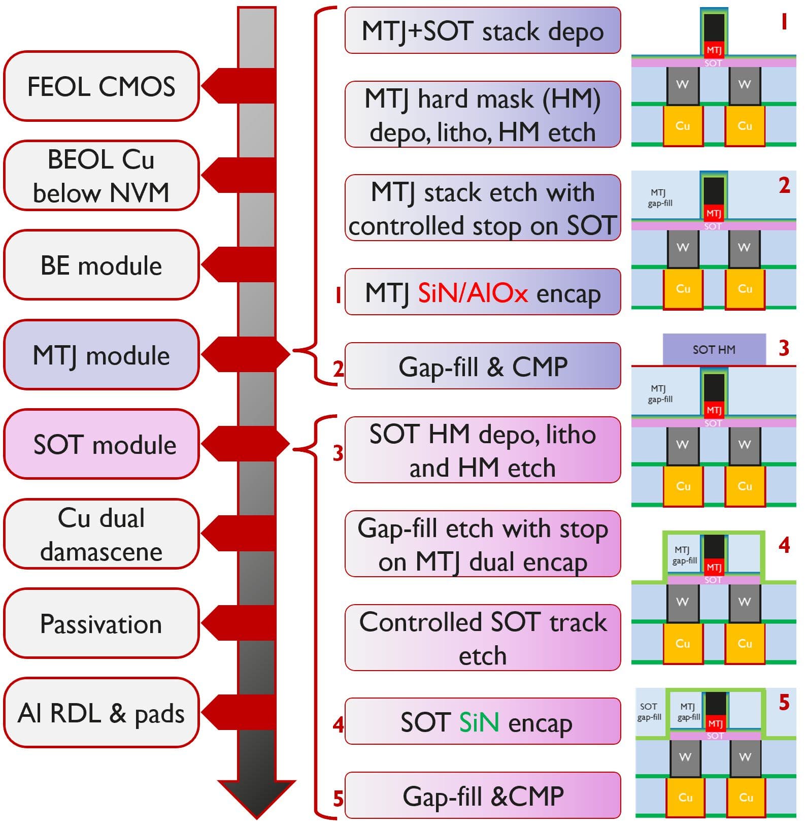
Figure 5 – Process flow for perpendicular SOT-MRAM integration, with dual SiN + AlOx encapsulation.
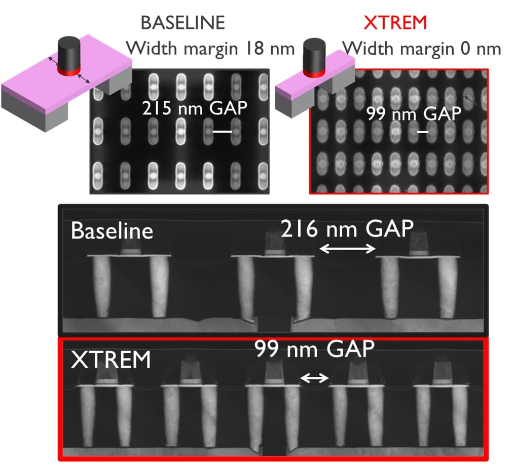
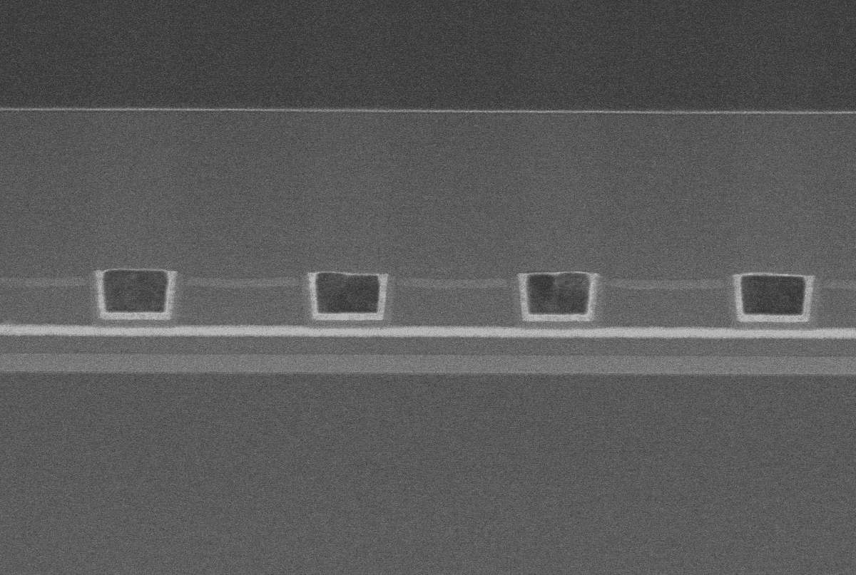
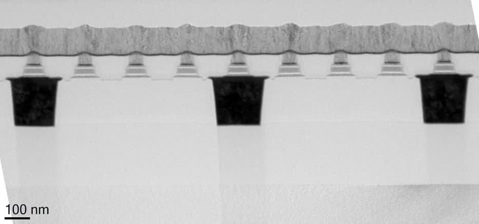
Figure 6 – SEM top view and TEM of baseline (black) and extremely scaled (red) SOT-MRAM devices (as presented at VLSI 2024 [9]).
Integrating MRAM devices into large arrays comes with an added complexity: all these thousands or even millions of bit cells must respond identically to the uniformly operating transistors in the peripheral circuit. Imec is currently exploring the knobs that make these devices less variable.
Conclusion
SOT-MRAM devices have been identified as potential candidates to replace SRAM in last-level cache applications. Imec addressed some of the remaining challenges, bringing the technology closer to real-world specifications. A re-design of the MTJ material stack led to more reliable switching at the device level and greater robustness against external magnetic influences. A complementary study of magnetic immunity revealed useful insights into how to protect devices from external magnetic fields. Finally, the demonstration of a functional array presents a milestone on the road to industrial uptake.
This article was originally published in EETimes.
Want to know more?
[1] ‘SOT-MRAM 300mm integration for low power and ultrafast embedded memories’, K. Garello et al., 2018 IEEE Symposium on VLSI Circuits;
[2] ‘Recent progress in spin-orbit torque magnetic random-access memory’, V. D. Nguyen et al., npj Spintronics 2, 48 (2024). https://doi.org/10.1038/s44306-024-00044-1;
[3] ‘First demonstration of field-free perpendicular SOT-MRAM for ultrafast and high-density embedded memories’, K. Cai et al., IEDM 2022;
[4] ‘Novel SOT-MRAM architecture opens doors to high-density last-level cache memory applications’, imec Reading Room article 2023;
[5] ‘Advancement in perpendicular SOT-MRAM technology for low power and high density embedded applications’, S. Van Beek et al., IEDM 2023;
[6] ‘Imec’s extremely scaled SOT-MRAM devices show record low switching energy and virtually unlimited endurance’, imec press release 2023;
[7] ‘Achieving 1ppm write-error rate in SOT-MRAM with synthetic antiferromagnetic free layer’, V.D. Nguyen et al., IEDM 2024;
[8] ‘Magnetic immunity of STT-MRAM: external magnetic field orientation impact on writing reliability’, N. Vander Meeren et al., IEDM 2024;
[9] ‘Extremely scaled perpendicular SOT-MRAM array integration on 300mm wafer’, F. Yasin et al., VLSI 2024.

Farrukh Yasin is a Principal Member of Technical Staff in the process integration department at imec. He joined imec in 2014 after graduating with an M.Sc. in engineering from KU Leuven. His responsibilities include design & process integration of test chips to explore new & emerging memory concepts. His interests cover a broad range of memory domains, from extending DRAM & NAND roadmaps, to emerging concepts in magnetic & ferroelectric memories, as well exploratory ideas like DNA & liquid memories. He is also passionate about the sustainability of the semiconductor industry, covering the analysis of GHG emissions & environmental footprint of memory technologies within the framework of sustainability program (SSTS) at imec

Van Dai Nguyen is a Senior Researcher specializing in magnetic devices at imec. He earned his Ph.D. in Nanophysics from the University of Grenoble Alpes, France, in 2012. Following a postdoctoral fellowship focused on magnetic domain wall and MRAM devices at the Neel Institute and Spintec in Grenoble, he joined imec in Leuven in 2018. Currently, he leads research on the large-scale integration of Spin Orbit Torque MRAM on 300 mm wafers for memory applications.

Dr. Siddharth Rao received his doctoral degree in electrical engineering from the National University of Singapore (NUS) in 2014, where he worked on enabling novel characterization methodologies for alternative write concepts such as microwave-assisted magnetic recording (MAMR) in the drive towards high density hard disk drive (HDD) technology beyond 10 Tb/in2. He joined imec in 2015 as a researcher in MRAM technology development. Currently, he is a Principal Member of Technical Staff and Team Leader of the magnetic devices team. In this role, he leads a team of researchers focused on accelerating the technology readiness level of different MRAM technologies, developing novel spintronic device concepts for next-generation memory, compute, and neuromorphic applications.

Gouri Sankar Kar received his Ph.D. in semiconductor device physics from the Indian Institute of Technology, Kharagpur, India, in 2002. From 2002 to 2005, he was a visiting scientist at the Max Planck Institute for Solid State Research, Stuttgart, Germany. In 2006, he joined Infineon/Qimonda in Dresden, Germany, as lead integration engineer and was responsible for vertical transistor development for the DRAM application. In 2009, he joined imec, Leuven, Belgium, where he is currently working as the VP R&D Compute & Memory Device Technologies
Published on:
16 December 2024


