A novel DRAM memory cell with two IGZO-based transistors
The bit cell of dynamic random-access memory (DRAM), the main memory within traditional compute architectures, is conceptually very simple. It consists of one capacitor (1C) and one silicon (Si)-based transistor (1T). While the capacitor’s role is to store a charge, the transistor is used to access the capacitor, either to read how much charge is stored or to store a new charge.
Over the years, bit cell density scaling allowed the industry to introduce subsequent generations of DRAM technology and cope with the growing demand for DRAM. But since about 2015, DRAM memory technology has struggled to keep pace with the performance improvement of the processor’s logic part: scaling, cost, and power efficiency issues form the building blocks of a rising ‘memory wall’. The large capacitor constrains scalability and 3D integration of the 1T1C bit cell, the ultimate path towards high-density DRAM. In addition, as the access transistor gets smaller, it provides an increasingly large leakage path for the capacitor’s charge to drain away. This lowers the data retention time and requires DRAM cells to be refreshed more frequently – impacting the power consumption.
In 2020, imec reported a novel DRAM bit cell concept that can solve these two issues in one go: a bit cell made up of two thin-film transistors (2T, one for read, one for write) and no capacitor (0C) [1]. The conduction channel of the thin-film transistors is composed of an oxide semiconductor, such as indium-gallium-zinc-oxide (IGZO). Due to its wide bandgap, IGZO-based transistors have an extremely low off current, benefitting the memory’s retention time, refresh rate, and power consumption. The longer retention time also relaxes the requirement for the storage capacitance, allowing the parasitic capacitance of the read transistor to take over the role of the storage element.
In addition, fabricating an IGZO 2T0C bit cell is simpler and more cost-effective than traditional cells. Other than Si, IGZO material can be deposited at relatively low temperatures, making it compatible with back-end-of-line (BEOL) processing. This opens doors to new DRAM architectures. First, it allows the DRAM periphery – the logic transistors that enable the full functionality of the DRAM chip – to be moved under the DRAM memory array instead of residing next to it. This reduces the footprint of the DRAM memory chip and makes connections between the array and periphery more efficient. In this configuration, the 2T0C DRAM bit cells are integrated into the peri’s BEOL, which is allowed by the properties of the IGZO material.
Second, the novel bit cell paves the way for stacked configurations, providing an additional increase in density. Either ‘2D’ or ‘true 3D’ stacking can be envisioned. With 2D stacking, several layers with ‘planar’ DRAM memory arrays are stacked on top of each other. With 3D stacking, the transistors that make up the 2T0C bit cell are stacked and monolithically integrated into vertically aligned plugs inspired by 3D NAND technology. The ability to deposit IGZO conformally in these high-aspect-ratio plugs, enabled by the technique of atomic layer deposition (ALD), is a key enabler of this 3D structure. These stacked configurations will help tear down the memory wall, allowing DRAM memories to continue playing a crucial role in data-intensive applications such as cloud computing and artificial intelligence. Implementing the two transistors on different levels (stacked 2T0C) has an additional benefit. A low-off-current oxide semiconductor channel is only fundamental in the write transistor to ensure long retention. For the read transistor, on current is the critical parameter, as it drives the read time, and high-mobility channel materials can be considered. The two transistors can thus be optimized separately.
First ‘conceptual’ demonstration of an IGZO 2T0C DRAM bit cell
After pioneering the concept, imec provided the first experimental demonstration of a functional 2T0C DRAM cell at the 2020 IEEE International Electron Devices Meeting (IEDM) [1]. Thanks to a low (extracted) off current of 3x10-19A/µm, these first 2T0C DRAM cells exhibited a retention time >400s, about 1,000 times longer than typical DRAM refresh times. The results were obtained after scaling and optimizing IGZO-based thin-film transistors processed on 300mm wafers. Optimizations were directed towards suppressing the impact of oxygen and hydrogen defects, one of the main challenges for developing good-performing IGZO-based transistors. Optimized transistors with a 45nm gate length were then integrated into a 2T0C DRAM bit cell architecture, where the parasitic capacitance of the read transistor served as the storage element.

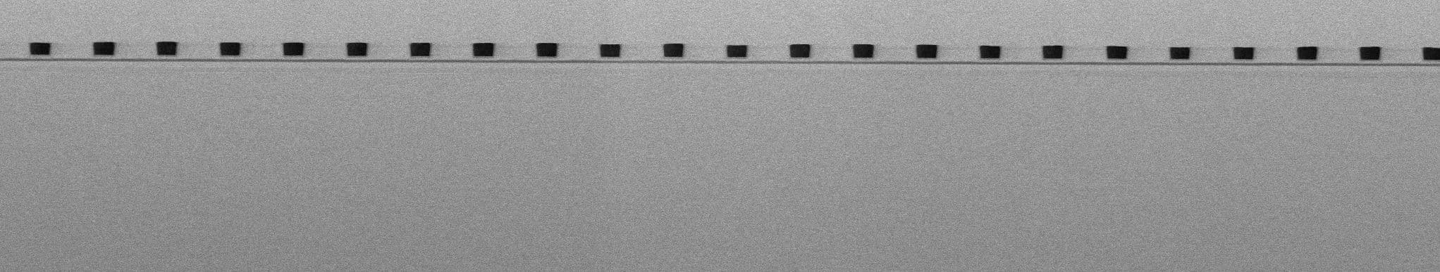
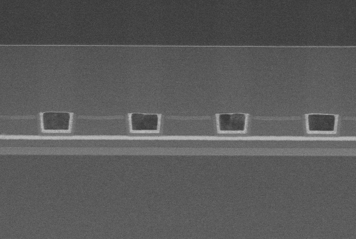
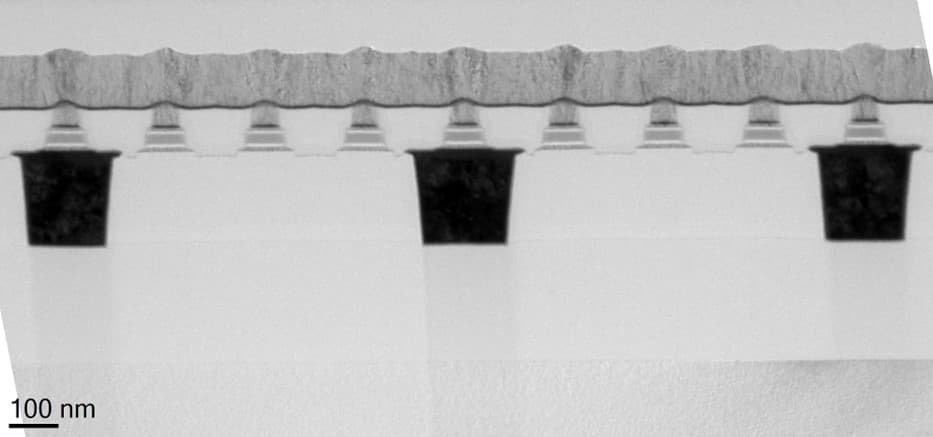
Figure 1 - (a) Layout of the 2T0C IGZO-based DRAM cell, with (b) corresponding TEM image (as presented at 2020 IEDM [1]). (W=write; R=read; WL=word line; BL=bit line.)
Do you want regular updates on imec’s semiconductor research?
Improving performance through bit cell engineering: an overview
Next, imec started to explore the knobs that allow the boosting of 2T0C DRAM density and improve performance and reliability metrics such as off current, data retention, endurance, on current, and threshold voltage (stability). In 2021 at IEDM, imec researchers presented a much-improved IGZO-based 2T0C DRAM bit cell with >1000s retention time and practically unlimited endurance (>1011 read and write cycles) with <10ns write time [2].
These breakthrough results followed an optimization of the IGZO transistor’s material stack and integration scheme: a gate-last approach with buried oxygen tunnel and self-aligned contacts combined with a scaled gate dielectric (Al2O3) thickness. Implementing the buried oxide tunnel in combination with an anneal in an O2 ambient reduced the oxygen-vacancy concentration in the IGZO channel, benefitting on and off currents.
This IGZO-DRAM technology set the stage for more aggressive DRAM scaling. The gate length of the IGZO transistor was scaled down to 14nm while still preserving >100s retention. The researchers also showed a variant of the 2T0C DRAM cell with much reduced IGZO layer thickness (5nm). This eliminated the need for an oxygen tunnel and O2 anneal step, leading to a simplified process flow. Imec also demonstrated functional transistors with conformally deposited thin IGZO channels (5nm, through ALD), a stepping stone towards 3D DRAM integration. [2]
More recently, imec used the reactive ion etch (RIE) technique instead of the commonly used ion beam etch (IBE) for patterning the active module of the 2T0C transistor. RIE allows for patterning at tiny dimensions (sub-100nm) with limited damage, further reducing area consumption. Moreover, using these transistors in 2T0C DRAM bit cells led to a much-improved retention time of >4.5 hours, thanks to an effective suppression of extrinsic leakage paths on the sidewalls of the transistor [3].
The potential of imec’s disruptive DRAM concept triggered interest from universities, research institutes, and companies worldwide. Several research groups started investigating other bit cell configurations, transistor performance ‘boosters,’ and alternative oxide semiconductor materials.
For example, IMECAS (Institute of Microelectronics of the Chinese Academy of Sciences), publishing about 2T0C IGZO DRAM since 2021, demonstrated an alternative 2T0C configuration to benefit multibit operation [4]. Later, they were the first to show transistors with a vertically integrated IGZO channel. The ability to monolithically stack the ‘vertical’ read and write transistors enables area-efficient 4F2 2D DRAM cell configurations (F being the minimum feature size for a given technology node) [5]. Macronix also implemented a 3D 2T0C bit cell with gate-around (GA) and channel-all-around (CAA) IGZO FETs [6]. Peking University optimized IGZO transistors based on material stack engineering, which enhanced 2T0C DRAM cell performance [7].
Thin-film transistors with oxide semiconductor channel materials other than IGZO are also being considered. One promising material is W-doped indium oxide (IWO), as showcased by Notre Dame University [8]. Stanford University initially considered indium-tin-oxide (ITO) for 2T0C implementation [9]. In 2024, in collaboration with TSMC, they also used IWO to build an n-type thin-film transistor. In addition, they were the first to combine the IWO n-type transistor with a p-type transistor also made of an oxide semiconductor (tin-oxide (SnO) in this case) for improved performance and reduction of coupling effects [10]. Most oxide semiconductor transistors are inherently n-type, which is why 2T0C DRAM bit cells usually implement two n-type transistors, for reading and writing.
The path to industry-viable IGZO-based 3D DRAM
2T0C IGZO-DRAM has recently been added to the long-term DRAM technology roadmap, according to a 2024 report of Yole Intelligence. The technology is envisioned as one of the possible approaches toward a much-desired 3D DRAM. Moreover, the demand for AI on edge devices is expected to surge in the coming years, generating the need for high-density embedded DRAM (eDRAM). The capacitor-less IGZO-DRAM technology is a very attractive candidate for this application. Building on its pioneering activities, imec started developing BEOL-compatible eDRAM implementations.
Yet, one key concern has made the memory industry hesitant to adopt IGZO-based DRAM technology: reliability. The n-type IGZO transistors mainly degrade because of the positive bias temperature instability (PBTI), which is manifested as an undesirable shift of the device threshold voltage and a decrease in the drain current. Worrisome is the hydrogen-related contribution to PBTI, a problem less familiar to the chip industry. Through the years, imec has made considerable progress in assessing, understanding, and modeling reliability failure, paving the way to building reliable IGZO transistors with a target lifetime of five years [11,12].
This work has been enabled in part by the NanoIC pilot line. The acquisition and operation are jointly funded by the Chips Joint Undertaking, through the European Union’s Digital Europe (101183266) and Horizon Europe programs (101183277), as well as by the participating states Belgium (Flanders), France, Germany, Finland, Ireland and Romania. For more information, visit nanoic-project.eu.
This article was originally published in Nature Reviews Electrical Engineering.
Want to know more?
[1] A. Belmonte et al. Capacitor-less, long-retention (>400s) DRAM cell paving the way towards low-power and high-density monolithic 3D DRAM. 2020 IEEE International Electron Devices Meeting.
[2] A. Belmonte et al. Tailoring IGZO-TFT architecture for capacitorless DRAM, demonstrating >103s retention, >1011 cycles endurance and Lg scalability down to 14nm. 2021 IEEE International Electron Devices Meeting.
[3] A. Belmonte et al. Lowest IOFF<3x10-21A/µm in capacitorless DRAM achieved by reactive ion etch of IGZO-TFT. 2023 Symposium on VLSI Technology and Circuits.
[4] K. Chen et al. Improved multi-bit statistics of novel dual-gate IGZO 2T0C DRAM with In-cell VTH compensation and ∆VSN/∆VDATA boosting technique. 2023 IEEE International Electron Devices Meeting.
[5] F. Liao et al. Novel 4F2 multi-bit dual-gate 2T0C for high-density DRAM with improved vertical-channel IGZO TFTs by self-aligned single-step process. 2024 IEEE International Electron Devices Meeting.
[6] F.-M. Lee et al. Bit-Cost-Scalable 3D DRAM Architecture and Unit Cell First Demonstrated with Integrated Gate-Around and Channel-Around IGZO FETs. 2024 Symposium on VLSI Technology and Circuits.
[7] Q. Hu et al. Optimized IGZO FETs for capacitorless DRAM with retention of 10 ks at RT and 7 ks at 85°C at zero Vhold with sub-10ns speed and 3-bit operation. 2022 IEEE International Electron Devices Meeting.
[8] H. Ye et al. Double-gate W-doped amorphous indium oxide transistors for monolithic 3D capacitorless gain cell eDRAM. 2022 IEEE International Electron Devices Meeting.
[9] S. Liu et al. Gain cell memory on logic platform – device guidelines for oxide semiconductor transistor materials development. 2023 IEEE International Electron Devices Meeting.
[10] F. F. Athena et al. First demonstration of an n-p oxide semiconductor complementary gain cell memory. 2024 IEEE International Electron Devices Meeting.
[11] A. Chasin et al. Understanding and modelling the PBTI reliability of thin-film IGZO transistors. 2024 IEEE International Electron Devices Meeting.
[12] A. Chasin et al. Unraveling BTI in IGZO devices: impact of device architecture, channel film deposition method and stoichiometry/phase, and device operating conditions. 2024 IEEE International Electron Devices Meeting.