This article was originally published in EDN (Part I and Part II).
NAND flash: the industry’s workhorse for data storage applications
For several decades, NAND flash has been the primary technology for low-cost and large-density data storage applications. This non-volatile memory is present in all major electronic end-use markets, such as smartphones, servers, PCs, tablets, and USB drives. In the conventional computer memory hierarchy, NAND flash is located the furthest away from the central processing unit (CPU). It's known to be relatively cheap, slow, and dense compared to static random-access memory (SRAM) and dynamic RAM (DRAM).
The significance of the flash memory segment is reflected by its impressive share in the global semiconductor capital expenditure (capex), where it accounts for about one third. Its success is related to its ability to continuously scale storage density and cost – the main drivers for NAND flash technology development. About every two years, the NAND flash industry has been able to substantially improve bit storage density, expressed in terms of increasing Gbit/mm2.
Along the road, several technology innovations have been introduced to maintain this trendline. Until recently, NAND flash memory cells were arranged in a planar configuration, using floating gate transistors for their memory operation. A floating gate transistor consists of two gates: a floating gate and a control gate. The floating gate is isolated from the rest of the transistor structure. It's usually made of polysilicon. The control gate is an ‘ordinary’ transistor gate.
Writing of the memory cell is accomplished by applying a pulse to the control gate. This forces electrons in (or out) of the floating gate – based on a tunneling mechanism. The presence (or absence) of charges alters the transistor’s threshold voltage. This shift is referred to as the memory window. Information is thus encoded in the threshold voltage of the floating gate transistor. And reading is done by measuring the drain current. The charges stored in the isolated gate remain unchanged for long periods of time. This gives the memory its non-volatile character.
Figure 1: Schematic representation of a floating gate cell.
Do you want regular updates on imec’s semiconductor research?
Floating gate has been the common approach for 2D NAND for over 20 years. It offers reliable operation despite its rather complex structure. Bit storage density improvement has been enabled by reducing the dimensions of the floating gate cell. 2D NAND scaling however, is saturated at about 15nm half pitch, mainly because of array reliability and electrostatic interference issues [1].
Going 3D to lower cost per bit
A further increase in bit storage density was brought about by transitioning to the third dimension. Not by stacking 2D-NAND-like layers, because the number of process steps that would be required to do so would dramatically add to the cost. The basic idea behind ’true’ 3D NAND is to stack cells to form a vertical string, thus reaching a higher density per unit area. In this configuration, cells are still addressed by horizontal word lines.
The most common fabrication approach, the gate-all-around (GAA) vertical channel method, starts with growing an oxide/(sacrificial-)nitride (word-line) layer stack. Next, cylindrical holes are formed by drilling down through the stack using advanced dry etch tools. Tunneling and trapping layers are deposited along the sidewalls of the hole. To complete this ‘punch and plug’ process, a thin polysilicon channel is deposited within the hole. And this is followed by a core filler to form a macaroni-like construct. In a next step, nitride is removed and replaced by the word-line metal. In these GAA structures, the cylindrical gates wrap around the channel structure. This enhances carrier injection into the trapping layers. And thereby enlarges the program/erase window.
Figure 2: representation of a typical 3D NAND flash structure (BL=bit line; WP=word plate; BSP=bottom select plate; SP=source plate; TSL=top select line) [2].
By adding more layers instead of shrinking feature sizes, the NAND flash industry abandoned the classical way of scaling. First commercial 3D-NAND products were introduced in 2013, with stacks counting 24 word-line layers (128Gb). Depending on the supplier, variations in the structure exist, known by different names such as V-NAND and BICS. As such 3D-NAND has been the first and (so far) sole technology to bring true 3D products to market. In the years to follow, many more layers have been put on top of each other to maintain the bit density scaling trendline. Recently, some of the major players introduced 176-layer 3D-NAND-based products, and this trend of increasing layers is expected to continue in the years to come.
From floating gate to charge trap
Along the road, additional innovations have been implemented to either facilitate the challenging 3D process or allow a further increase of the bit density. An example of the latter was an increase of the number of up to 4 bits per cell. This is a true asset of NAND flash technology. With 4 bits, for example, the multi-level cells use 16 discrete charge levels in each individual transistor, enabled by the sufficiently large memory window.
Another notable innovation was the replacement of the floating gate cell by a charge trap cell, which involves a more simplified process flow. The working principle of both cell types are relatively similar. But in a charge trapping cell, the trapping layer is an insulator – usually silicon nitride. This provides less electrostatic interference between neighboring cells. Such a charge trap cell is now the base of most 3D NAND structures.
Towards increasing bit storage densities
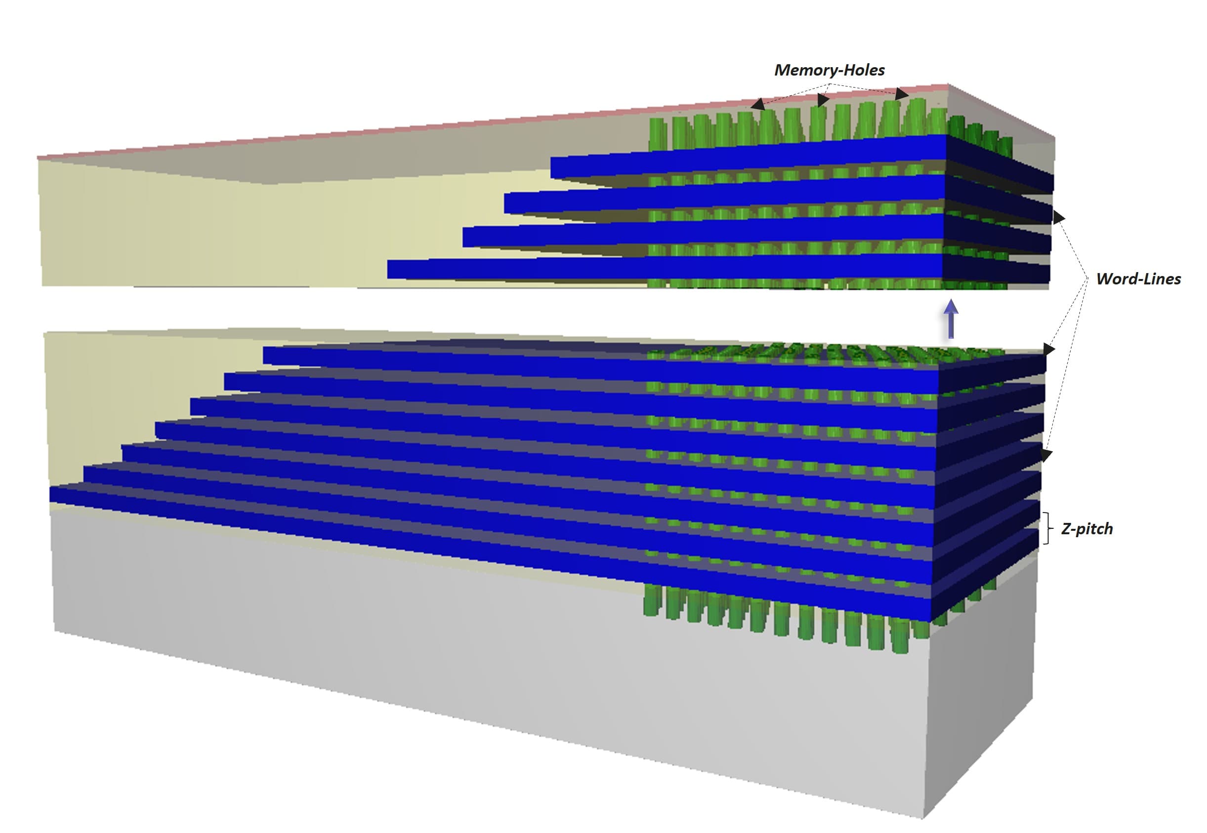
To maintain the NAND flash roadmap, some major players recently announced a further increase of the number of layers to 500 or more. Following the trendline, this number will increase to 1,000 before the end of the decade [3]. Increasing the number of layers introduces ever higher processing complexities. It challenges deposition and etch processes and causes stress to build up inside the layers. To address some of these challenges, NAND fash makers recently began splitting up the number of layers into two (or more) tiers. And stacking the individually processed tiers on top of each other.
There is, however, a growing concern that without major innovations this evolution will gradually reduce the cost efficiency of the NAND flash storage products. The increase in layer count requires an investment in highly advanced deposition and etch tools. And the trend of stacking multiple tiers will dramatically add to the mask count, and number of processing steps and time. It could also cause the storage roadmap to slow down, with stacks of 1,000 layers being unavailable until 2030.
As layer count increases, there is pressure to shrink the layer thickness and control the height of the stack for patterning and stress reasons. This z-pitch scaling involves a reduction of the height of all materials that are involved in the stack. Those include word-line metals and oxides, which each bring along specific challenges.
Z-pitch scaling is likely to be complemented by a further reduction in x-y dimensions as well. This would require major innovations in the memory unit cell, which has remained unchanged during the years of 3D NAND development. Therefore, new materials and cell architectures are being explored as alternatives for today’s GAA NAND flash cell.
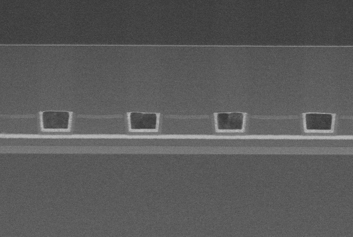
One notable development is a trench-like architecture to connect the transistors. In this architecture, the memory cells are no longer circular. They are implemented at the sidewall of a trench, with two transistors at opposite ends of the trench. This significantly increases bit density. From an operation point of view, this trench cell resembles a planar unit cell (being put upright) compared to the circular GAA NAND flash cell. Although it comes with a slight penalty in electrical characteristics (such as the program/erase window), the unit cell area in a trench-like configuration can be reduced in the x-y direction compared to a ‘GAA’ cell [3]. As such, the trench cell is put forward as a next generation NAND flash cell architecture. It's expected to reduce the x-y pitch from today’s 140nm (effective) to about 30nm.
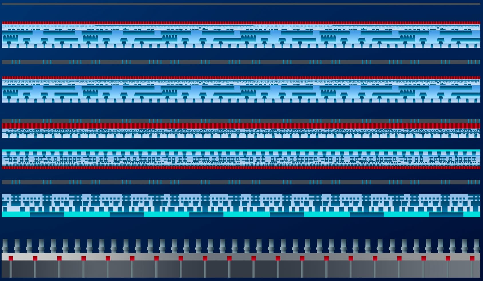
Figure 3: (top) gate-all-around vs. (bottom) trench NAND flash cell architecture.
In a more distant future, we expect that more disruptive ‘post-NAND’ innovations (such as imec’s liquid-based concepts) will be needed to continue the density scaling trendline and enter the terabit/mm2 era.
Imec to push the GAA NAND flash roadmap to its ultimate limits
Relying on a long track record in 2D and 3D NAND flash technology development, part of imec’s storage R&D activities focus on continuing the conventional GAA 3D-NAND-fash scaling roadmap. By both modeling and experimenting, the team explores innovations in elementary 3D NAND cells to allow for a further reduction in x-y-z dimensions. With the modeling and simulation work, they investigate the impact of introducing new materials and architectures on the electrical performance of the NAND flash memory cells. Modeling also allows the team to enhance fundamental understanding, and to identify and mitigate 3D NAND flash cell scaling roadblocks. The experimental work is structured around a test vehicle with a limited number of layers (typically three to five, 300nm in height). This is relevant for studying the effects of scaling on the electrical memory cell metrics.
A view on recent insights and achievements
A z-shrink of the NAND flash layer stack involves squeezing the materials that are used for creating the word-line layers, including the word-line metal. Currently, vertical word-line pitches in commercial 3D-NAND products range between 50 and 60nm. And tungsten (W) is the word-line metal of choice. It also acts as a gate electrode for the NAND-fash memory cell and is integrated in the stack by a replacement metal gate process.
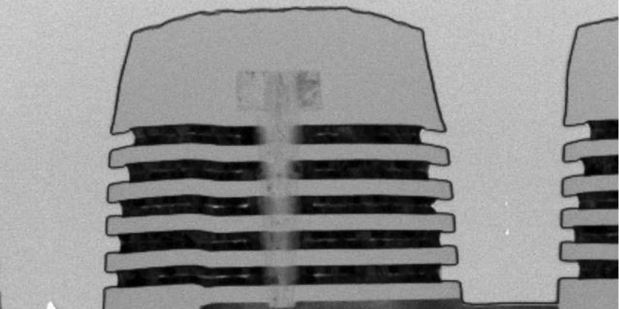
Reducing the word-line metal thickness comes along with an unwanted resistivity increase. This enhances resistance-capacitance (RC) delay and slows down access times. Imec, therefore, is looking at alternative metals such as Ru and (barrierless) Mo with potentially lower resistivity at small dimensions. At the 2021 IEEE Symposium on VLSI Technology and Circuits (VLSI 2021), the team demonstrated improved resistivity and memory characteristics for Ru and Mo word lines down to a record low 40nm word-line pitch. [4,5]
![Figure 4: TEM cross-section of Mo integrated in a 5-stack 3D-NAND with scaled word lines down to 40nm pitch [5].](/_next/image?url=https%3A%2F%2Fdrupal.imec-int.com%2Fsites%2Fdefault%2Ffiles%2F2022-04%2FFigure%25204%2520-%2520TEM%2520Mo%2520word%2520lines.jpg&w=3840&q=75)
Figure 4: TEM cross-section of Mo integrated in a 5-stack 3D NAND with scaled word lines down to 40nm pitch [5].
The team also explores alternative materials for the charge trap layers, the tunnel dielectrics and the metal gate stack. And it investigates their impact on memory performance. For example, they investigated how high-work-function metals in combination with a thin high-k liner can improve the 3D NAND erase operation. [6,7]
In today’s GAA 3D NAND fash structures, the channel material used is polysilicon. Depositing the polysilicon material in the ‘plug’ that runs through the material stack is considered the most cost-effective way to fabricate the devices. But as the number of layers increases, the inherently defect-rich polysilicon channel deteriorates the device read current. Imec, therefore, explores ways to improve channel mobility. It does this in two ways: by introducing alternative channel materials or improving the quality of the polysilicon channel.
At the 2021 IEEE International Electron Devices Meeting (IEDM 2021), the team presented the results of using metal-induced lateral crystallization (MILC) in a 3D test structure to boost the polysilicon channel quality. MILC is a process in which amorphous silicon transforms into a crystalline state at relatively low temperatures, catalyzed by the presence of a metal such as Ni. They concluded that it is possible to achieve up to 10 times higher mobility and enhanced channel control with an improved MILC process – compared to a regular polysilicon channel [8].
Modeling work focuses, for example, on understanding the non-ideal programming efficiency of charge trap layer flash memories. This inefficiency is reflected in the slope of the incremental step pulse programming (ISPP) curve. And it results in a higher required programming voltage. The team recently gained a better understanding of this poorly understood phenomenon. At IEDM 2021, researchers outlined different contributions to the ISPP slope and proposed ways for mitigation. For example, by using a high-k dielectric within the charge trap layer cell [9].
Figure 5: contribution of carrier injection (inj), escape (esc) factors and trap filling on ISPP curve (top) and slope (bottom) [9].
Other modeling work focuses on the impact of introducing new materials and architectures (such as the trench cell) on the mechanical stress within the layer stack. Mechanical stress is known to introduce wafer warpage, local pattern deformation, and cracks within the 3D NAND flash structure. At the 2021 IEEE International Interconnect Technology Conference (IITC 2021), imec presented a finite-element modeling (FEM) approach that can be used to evaluate and mitigate wafer warpage in future 3D-NAND memory fabrication. All without needing to experimentally build a >100-layer stack [10].
3D NAND flash to tap into new market segments
Today, 3D NAND flash technology is used in high-density, low-cost data-heavy storage applications such as solid-state drives. But the technology is increasingly finding its way into other markets, particularly the low(er)-latency storage segment. Here, it can potentially serve a range of storage applications that require faster read access time than traditional NAND flash. An example is that of applications such as look-up tables for databases. This faster variant of NAND flash will enter the storage class memory (SCM) space. This should help close the gap between fast, volatile DRAM and slow, non-volatile 3D NAND flash.
Low-latency storage applications will require shorter read access times than conventional high-density 3D NAND flash. Several routes are available to make that possible. One way is to revert to single-bit memory cells. This mainly improves program speed (~30us) to approach read speed (~10us). Further optimizations of the design space may involve reducing the word-line lengths or altering the RC-delay parameters. With these and other measures, NAND flash technology is expected to enter the low-latency storage market with read access times in the order of 10µs. [11]
Low-latency storage: a major role for FeFET
In the longer term, much is expected of ferroelectric memories to fulfill this role. More particularly from memories based on the 3D ferroelectric field effect transistor (3D-FeFET). 3D FeFETs are expected to outperform 3D NAND flash in terms of speed. This makes them ideal candidates for low-latency storage.
Figure 6: An imec view on the data storage roadmap.
The architecture of a FeFET is similar to that of a traditional n-channel MOS transistor. In a FeFET, the gate dielectric has been replaced by a ferroelectric material (such as HfO2 in its orthorhombic crystal phase). A ferroelectric can be in two electrical polarization states. These can be reversed through an external electric field – provided by applying a pulse to the transistor gate. After the field is removed, they retain their polarization state. This gives the material its non-volatile characteristic.
The two stable, remnant polarization states of the gate insulator modify the transistor threshold voltage. The binary states are thus encoded in the threshold voltage of the transistor. The operating principle of a FeFET memory is very similar to that of NAND fash. Writing of the memory cell is completed by applying a pulse to the transistor gate. Reading is performed by measuring the drain current.
Just like NAND flash, FeFETs can be fabricated in a true 3D fashion by using a 3D NAND-like manufacturing flow [12, 13]. To build 3D-FeFETs, a trench-like architecture is preferred over a GAA-structure. This is because FeFETs do not benefit from circular charge carrier injection.
Although still in the early stage of R&D, 3D-FeFETs are expected to present some notable advantages compared to 3D-NAND. They are simpler to process, consume less power, and can potentially operate at much lower voltage, which benefits their reliability. Additionally, read and write access times in the order of a few µs are feasible, making them an attractive alternative to 3D-NAND for future low-latency applications.
Imec to optimize 3D FeFETs for low-latency storage applications
Imec is addressing the main challenges related to the processing, characterization, and reliability of 3D-FeFETs. Reseachers are exploring the best possible architecture, material combinations, and memory operating schemes (such as program/erase scheme) to optimize 3D-FeFETs for low-latency storage applications. To enter the (NAND side of) the SCM space, speed and cycling endurance (or the number of program/erase cycles before failure) are the most crucial parameters. While the cycling endurance of 3D NAND is limited to about 105, the team is working towards 107 cycling endurance for 3D-FeFET. This could already be demonstrated for planar FeFET architectures. A higher cycling endurance is expected to come along with a slight penalty in density and retention.
One approach towards improving cycling and speed is optimizing the channel material. Just like in NAND, the FeFET channel today is composed of polysilicon. But this material challenges FeFET operation. The combination with the ferroelectric HfO2 stimulates regrowth of an interfacial oxide layer. This creates unwanted trapping effects for the charge carriers and degrades the program/erase cycling performance of the memory. Besides looking into mitigation strategies, imec explores alternative channel materials, including oxide semiconductors. These channel materials should come with a low thermal budget to preserve the orthorhombic phase of the HfO2 (or other ferroelectric layers).
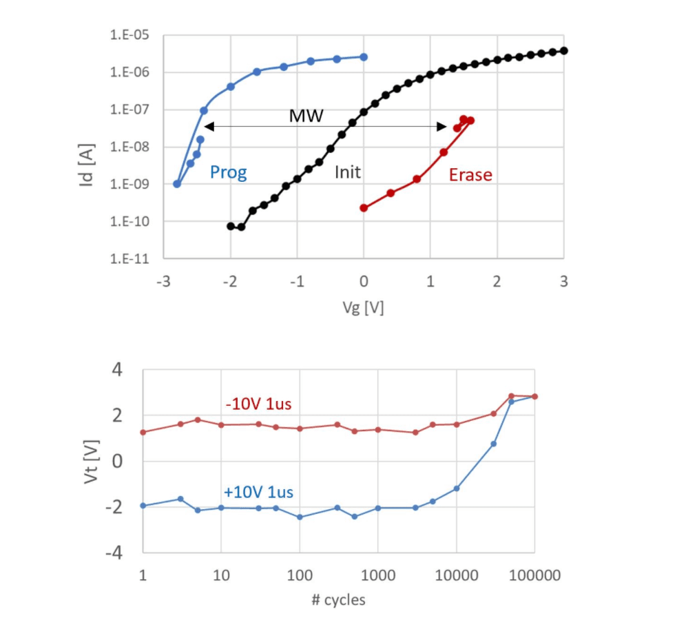
Figure 7: (top) memory window after applying 100ns program/erase pulses; (bottom) evolution of the threshold voltage VT with cycling after program and erase.
The orthorhombic crystal phase of HfO2 can be stabilized by using an optimal combination of dopants, strain and annealing. Today, mainly Si is used as a dopant atom, as it can keep the orthorhombic phase even at higher thermal budgets. The imec team also studies alternative dopants and doping conditions and explores other ferroelectric materials besides HfO2.
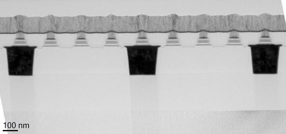
For the architecture, imec actively pursues the 3D trench architecture, of which a first test vehicle has been demonstrated.
Conclusion
While for decades NAND flash was aimed at high density storage applications, we now also see faster variants of the technology emerging – aimed at low-latency storage. For the latter application, imec sees an important role for 3D-FeFET in the further future. For both NAND and FeFET, imec explores novel materials and cell architectures, and studies their impact on memory performance. Besides, the team is gaining more insight into the main reliability degradation mechanisms. While innovations in 3D NAND flash aim at the continuation of the high-density storage roadmap, imec prepares 3D-FeFET for its future role in the low-latency storage market.
Want to know more?
[1] ‘Reliability of NAND Flash arrays: a review of what the 2-D–to–3-D transition meant’, C.M. Compagnoni, IEEE Transactions on electron devices, Vol. 66, n°11, Nov 2019;
[2] ‘Optimal Integration and Characteristics of Vertical Array Devices for Ultra-High Density, Bit-Cost Scalable Flash Memory’, Y. Fukuzumi et al., 2007 IEDM;
[3] ‘3-D NAND technology achievements and future scaling perspectives’, A. Goda, IEEE Transactions on Electron Devices, Vol. 67, n°4, April 2020;
[4] ‘Integration of ruthenium-based wordline in 3-D NAND memory devices’, L. Breuil et al., 2020 IMW;
[5] ‘First demonstration of ruthenium and molybdenum word lines integrated into 40nm pitch 3D-NAND memory devices’, A. Ajaykumar et al., 2021 VLSI;
[6] ‘Understanding the origin of metal gate work function shift and its impact on erase performance in 3D NAND Flash memories’, S. Ramesh et al., Micromachines 2021, 12, 1084;
[7] ‘Erase behavior of charge trap Flash memory devices using high-k dielectric as blocking oxide liner’, S. Ramesh et al, SISC20;
[8] ‘Understanding the kinetics of metal induced lateral crystallization process to enhance the poly-Si channel quality and current conduction in 3-D NAND memory’, S. Ramesh et al., 2021 IEDM;
[9] ‘Understanding the ISPP slope in charge trap Flash memory and its impact on 3D NAND scaling’, D. Verreck et al., 2021 IEDM;
[10] ‘Multi-scale modeling approach to assess and mitigate wafer warpage in 3-D NAND fabrication’, O. Orkut Okudur et al, 2021 IITC;
[11] ‘13.5 A 128Gb 1b/Cell 96-Word-Line-Layer 3D Flash Memory to Improve Random Read Latency with tPROG=75µs and tR=4µs’, T. Kouchi et al., 2020 IEEE International Solid- State Circuits Conference - (ISSCC), 2020, pp. 226-228, doi: 10.1109/ISSCC19947.2020.9063154;
[12] ‘3D memories and ferroelectrics’, J. Van Houdt, 2017 IEEE-IMW, Monterey, CA, invited, p. 92-94;
[13] ‘Vertical ferroelectric HfO2 FET based on 3D NAND architecture: towards dense low-power memory’, K. Florent et al., 2018 IEDM;

Maarten Rosmeulen received his M.Sc. degree in physics in 1993 and his M.Sc. degree in physics of micro-electronics and materials science in 1994, both from the KU Leuven, Belgium. In 2005, he received his Ph.D. in electrical engineering from the KU Leuven. Since then, he has been with imec, in Leuven, Belgium, where he has been active as an R&D engineer in process integration, semiconductor device design, and electrical device characterization for multiple internal and external projects. In 2009 he became a project leader in developing GaN-on-Silicon Light Emitting Diodes (LEDs). In 2014 he became the team leader of the Pixel Design and Testing team and has been responsible for the development of CMOS Image Sensor (CIS) technologies. In 2019 he became the program director of the Storage Memory program, the position he holds today.

Jan Van Houdt received a Ph.D. from the KU Leuven. During his PhD work, he invented the HIMOS™ Flash memory, which he transferred to several industrial production lines. In 1999, he became responsible for Flash memory at imec and, as such, was the driving force behind the expansion of imec’s Industrial Affiliation Program on Memory Technology. Jan has published over 300 papers in international journals and accumulated over 250 conference contributions (incl. ~50 invitations and five best paper awards). He has filed about 100 patents and served on the program and organizing committees of 10 major semiconductor conferences. In 2014, he received the title of IEEE Fellow for his contributions to Flash memory devices. In the same year, he started the Ferroelectrics program at imec and became a guest lecturer at the KU Leuven, teaching CMOS and memory technology. Today, he is a Program Director at imec, imec Fellow, and Professor at the Physics and Astronomy Department of the KU Leuven.
Published on:
5 April 2022

