Working in conjunction with her colleagues at imec as part of her doctorate research, Sofie Beyne has developed a new measuring method for detecting electromigration in the interconnection module (or back-end-of-line, BEOL) of chips. The new method sits alongside the standard method – according to Black’s Law – perfectly and also provides new capabilities for obtaining greater insight into the issues surrounding electromigration.
Electromigration: a worsening problem
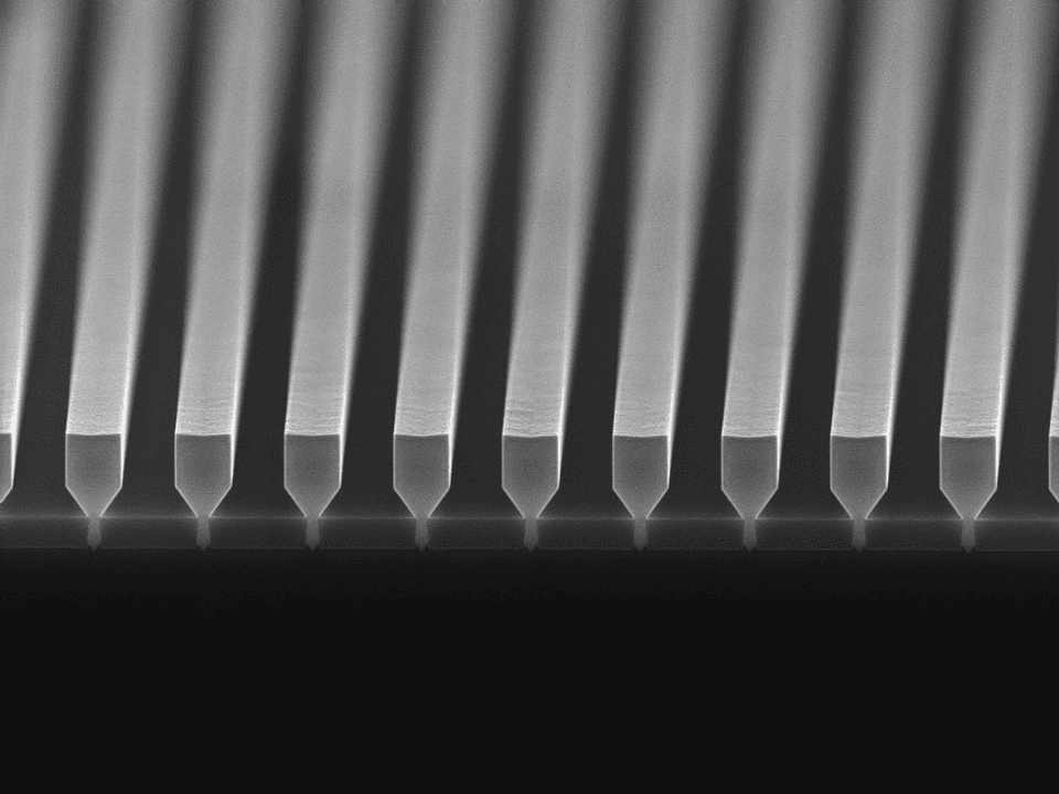
Electromigration in the BEOL of chips occurs in the metal (copper) pathways. Due to high current densities in these pathways, the copper atoms move and empty spaces or – just the opposite – accumulations are created. As a result, the copper pathways stop working (due to short-circuits) and the chips can even fail.
This phenomenon has been known for over 100 years. In fact, electromigration caused the early commercial chips to stop working after just 3 weeks. Fortunately, they last much longer these days, not because electromigration doesn’t occur any longer, but because the design of the circuit helps to get round the adverse effects of electromigration. Yet electromigration problems can still happen. At the beginning of the 1990s, electromigration made the news when the launch of a rocket from Cape Canaveral had to be aborted because the onboard computer had stopped working. Research revealed that the problem was caused by electromigration.
These days, electromigration is more relevant than ever. Because increasingly fine metal pathways are used now, resulting in higher current densities, there is more opportunity for electromigration to occur. The use of new metals also makes it important to study the phenomenon of electromigration in detail and to understand it properly before introducing the use of a new metal in the production of commercial chips.
The standard reliability test for electromigration consists of subjecting the circuit to a very high temperature (> 150°C) and current density (j> 1MA/cm2). By doing this, the occurrence of electromigration is accelerated. Black’s Law is then applied to extrapolate the life expectancy of the chip.
These ‘accelerated’ tests have various disadvantages. One of them is that different processes may possibly occur in the chip than would normally happen at normal temperatures and current densities, rendering predictions unreliable. These tests also require a great deal of time and are destructive for the chips. This means that no other tests can be carried out on the same chip afterwards (such as electrical tests).
Certainly with the use of new materials – including cobalt – standard tests can last for months, because very high temperatures and current densities are required before electromigration occurs.
The waterfall sound in chips
When a DC current is sent through a metal, small current fluctuations occur as the result of electron scattering. These small fluctuations can be measured in time and, using the Fourier transformation, converted to the frequency domain. That way, the power spectral density (PSD) can be calculated.
In metals, this power spectral density appears to follow the 1/f spectrum in the low frequency range. Why this is so we do not yet know. This sort of 1/f noise, also called ‘pink noise’, occurs in nature too, for example like the sound of a waterfall. Noise that follows both the 1/f and 1/f² spectrum is called low-frequency noise because with this kind of noise, the low frequencies sound louder than with high frequencies (in contrast to white noise, where all of the frequencies are the same).
Measuring low-frequency noise in chips is interesting because the noise suddenly appears to change when a phenomenon such as electromigration occurs. And there are various advantages associated with the new testing method based on this noise (compared with the standard method): the method is non-destructive and much faster (which is certainly important for new metals) – plus it provides greater insight into the nature and occurrence of electromigration (by using ‘ordinary’ temperatures, it is also more likely that the phenomenons observed are the same as the ones occurring under actual operating conditions for the chips).

At 300 minutes of electromigration stress, there is a change in the low-frequency noise. This can be attributed to the voids in the metal pathways resulting from electromigration.
New insights provided by a new measuring method
The new measuring method for electromigration is already being used by imec researchers and has provided a number of surprising insights. A first observation is that the activation energy for electromigration decreases when finer metal pathways are used. This has been studied for copper. When copper pathways become finer than 30 nm, there are many polycrystals present and so electromigration occurs more quickly as the result of diffusion at the edges of these crystals (grain boundary diffusion). In establishing design rules, the typical assumption is one activation energy for BEOL interconnections that are made from the same material, although it would be better to assume a lower activation energy with thinner pathways.
Second, with this new method, variations can be observed between different chips on a wafer. This could enable wafer maps to be produced, indicating the life expectancy for each chip – something that is not possible with the standard method.

Variability in the activation energy (defined by measuring the low-frequency noise) per chip on a wafer. This type of wafer map is not possible with standard tests for electromigration.
A third area of research for which the new test has been used is to test the electromigration reliability of Ruthenium metal being examined as an alternative for the copper pathways in the BEOL. Using the standard method, the test would take a very long time because these new materials have a long life expectancy and need to be exposed to very high temperatures and current densities before they fail. This means that determining the activation energy with traditional testing methods would be particularly time-consuming. But with the new test method, the activation energy can be determined fairly quickly.
Finally, the effect that various sorts of barriers have on electromigration has also been studied. For example, Ruthenium liners seem to have a positive effect on the electromigration resistance of copper interconnections, as does adding manganese to the seed layer.
New measuring method ready for use
In addition to imec researchers, partner companies and university research groups are also interested in using the new method to gain more insight into electromigration, as well as in possible adaptations that protect better against electromigration in new materials, etc.
For chip manufacturers, the method is of interest both for research and for production. In production it makes the ideal addition to the standard method, because it offers new possibilities, such as providing a deeper fundamental insight and predictions of the electromigration resistance of individual chips. For instance, ‘wafer maps’ can be measured, showing the variation in electromigration activation energy and defect concentration per chip. Chips with a higher activation energy and/or lower defect concentration will have a longer service life and so can be used for critical applications (such as space travel and automotive).
Being a PhD student at imec: bringing ‘academic’ research closer to industry
The work described above, was done in the framework of a PhD study. Imec works in conjunction with universities to give researchers the opportunity to conduct their work in a high-tech environment and state-of-the-art cleanroom. Imec’s international position and its network of partners also makes the environment it provides extremely interesting for carrying out research for a PhD. Sofie Beyne, for example, was given the opportunity to do two internships with imec partners. This enabled her to build up a great deal of experience in a short space of time. At the end of 2019 she will present her doctoral thesis and begin a job in the United States with a company that she was introduced to via the imec network.
More info on PhDs at imec can be found on this website.
Want to know more?
The papers listed below can be requested via our contact form.
- “1/f noise measurements for faster evaluation of electromigration in advanced microelectronics interconnections”, Journal of Applied Physics 2016
- “Study of the enhanced electromigration performance of Cu(Mn) by low-frequency noise measurements and atom probe tomography”, Applied Physics Letter 2017
- “Study of electromigration mechanisms in 22nm halfpitch Cu interconnects by 1/f noise measurements”, IITC 2017
Sofie Beyne is a PhD student at imec and KU Leuven, researching electromigration in nano-interconnects as part of the REMO-team. In 2015 she received a master’s degree in materials science and engineering from KU Leuven, which included a one-year exchange program at EPFL in Switzerland. Her work is financed by the fund for scientific research in Flanders (FWO).
Published on:
1 March 2019


