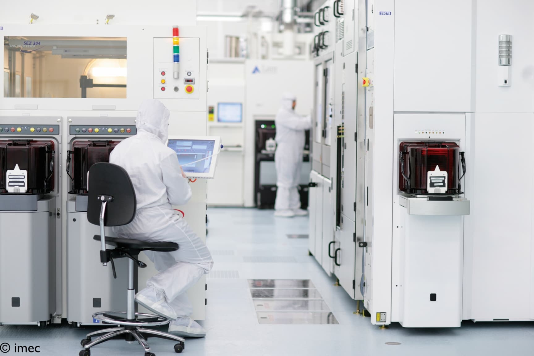
CMOS: advanced and beyond
Discover why imec is the premier R&D center for advanced logic & memory devices.
Integrated photonics
Take a look at technologies for optical transceivers, sensors and more.
Health technologies
See how imec brings the power of chip technology to the world of healthcare.
Sensing and actuation
Explore imec’s CMOS- and photonics-based sensing and actuation systems.
Connectivity technology
Look into our reliable, high-performance, low-power network technologies.
More expertises
Discover all our expertises.
Research
Be the first to reap the benefits of imec’s research by joining one of our programs or starting an exclusive bilateral collaboration.
Manufacturing
Go from idea to scalable and reliable semiconductor manufacturing with IC-Link.
Venturing and startups
Kick-start your business. Launch or expand your tech company by drawing on the funds and knowhow of imec’s ecosystem of tailored venturing support.
Education and workforce development
Imec supports formal and on-the-job training for a range of careers in semiconductors.
NanoIC pilot line
Aligned with the EU Chips Act, access to the pilot line will accelerate beyond-2nm innovation.

Press release
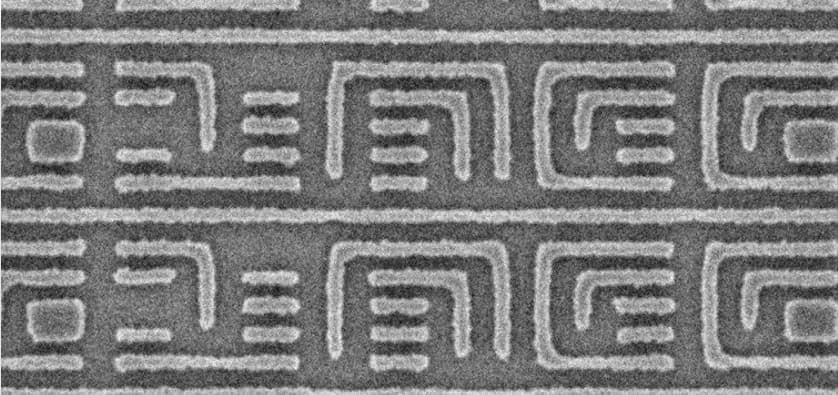
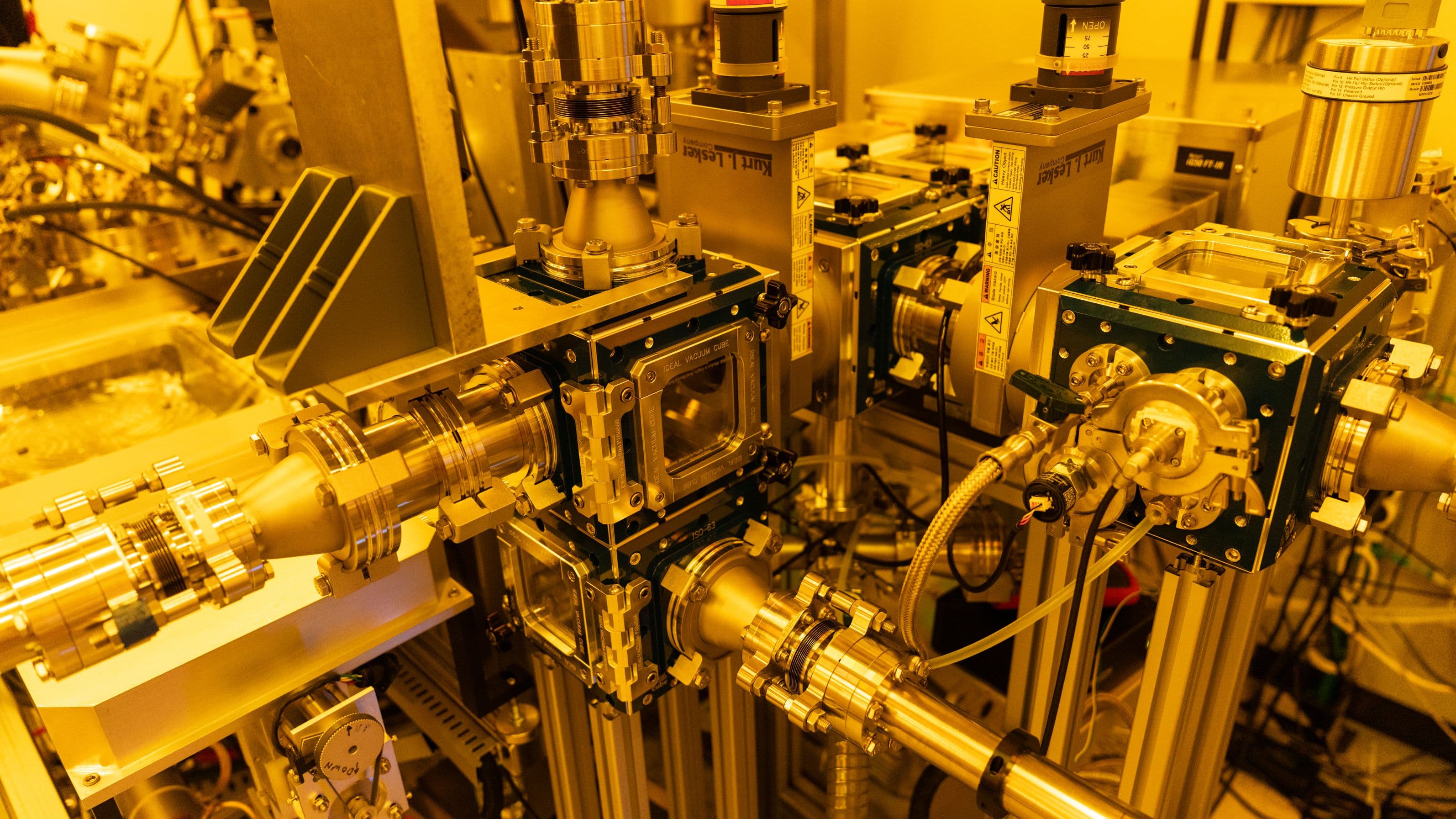
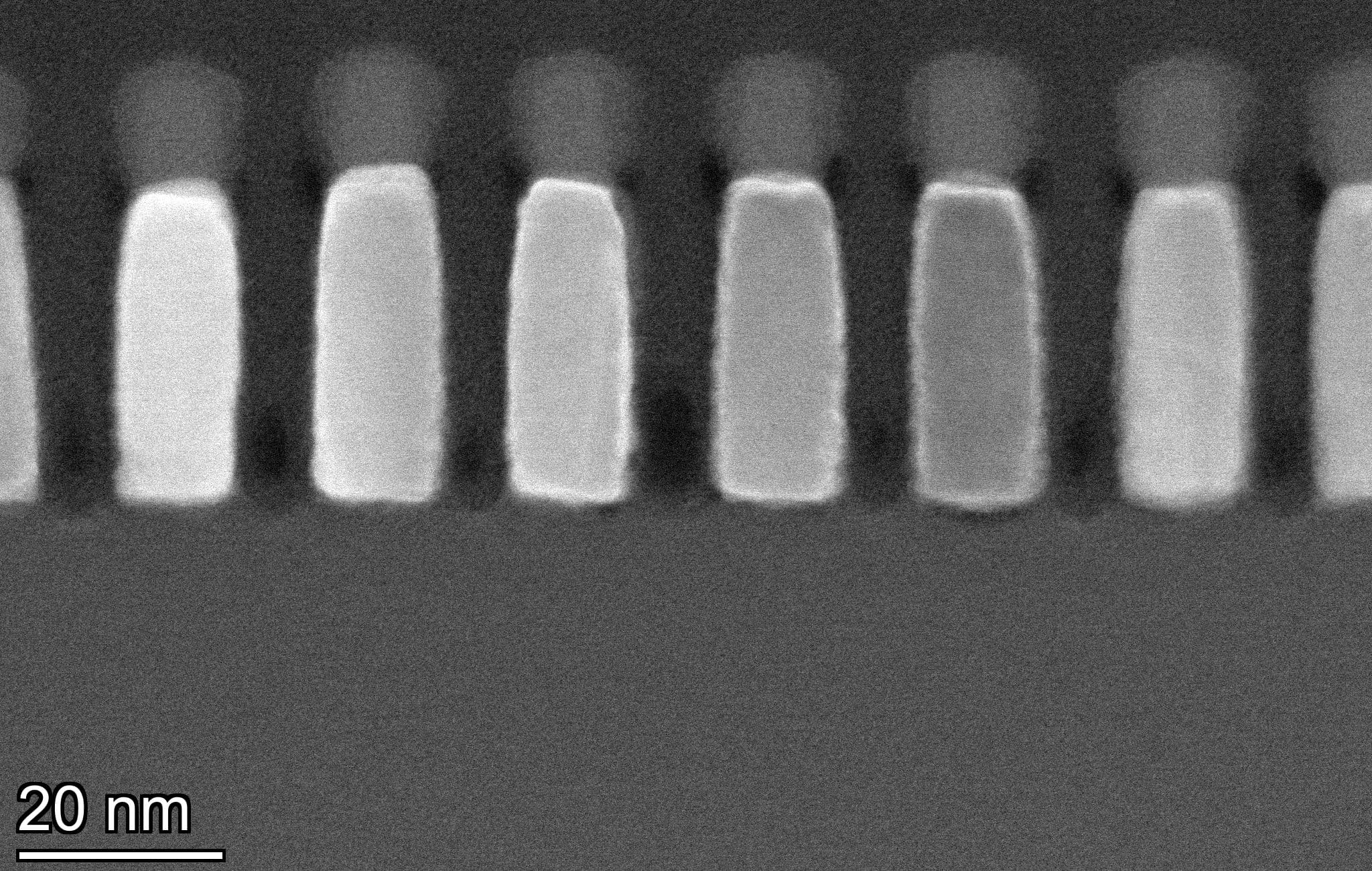
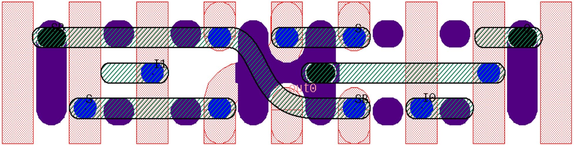
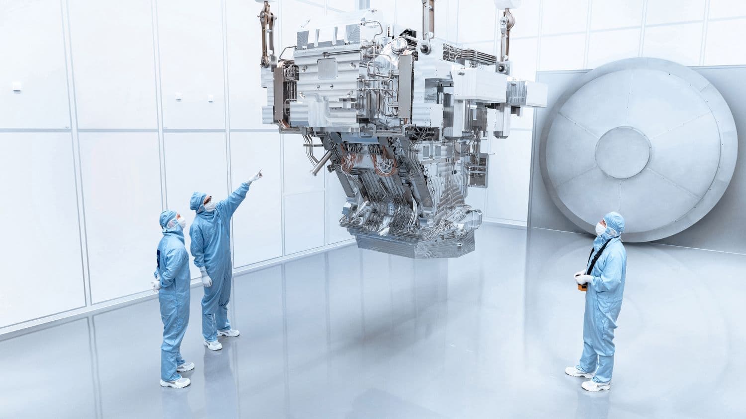
Imec demonstrates electrical yield for 20nm pitch metal lines obtained with High NA EUV single patterning
First electrical tests at 20nm pitch present a next milestone in validating the High NA extreme ultraviolet (EUV) patterning ecosystem