The Si-based logic scaling roadmap
It has been clear for nearly two decades that the pure dimensional scaling inspired by Moore’s Law is no longer the only indicator to predict the evolution of CMOS technology nodes. The first sign came around 2005 when node-to-node performance improvements at fixed power – referred to as Dennard scaling – started to slow down. Gradually, the semiconductor industry started to complement lithography-centric scaling with other technology innovations to maintain the performance-power-area-cost benefit: material and architectural explorations at transistor level, design-technology co-optimization at standard cell level, and system-technology co-optimization enabled by 3D integration technologies.
At transistor level, the scaling-induced performance degradation originated from short channel phenomena. The combination of strong gate length reduction and the shortening of the conduction channel led to an increase in leakage current, even when no voltage was applied to the gate. Similarly, the impact of source and drain on the shrinking channel region grew dramatically.
These short channel effects drove the chip industry to transition from planar MOSFET to FinFET, and recently, to gate-all-around (GAA) nanosheet transistors for high-performance computing applications. These architectural innovations allowed the gate to regain electrostatic control over the conduction channel. The nanosheet family of transistors promises to continue the logic scaling roadmap with at least three technology generations, when combined with innovations at standard cell level. These include, among others, advanced interconnect and middle-of-line schemes and the introduction of backside power delivery networks (BSPDNs).
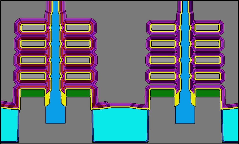
The complementary FET or CFET will be the next game changer, allowing further area reduction by stacking n and p channels on top of each other. Imec foresees its introduction from the A7 node onwards, extending the imec technology roadmap to at least the A3 generation. Just like in GAA nanosheet transistors, the gate – now common to n and p – fully wraps around and in between the Si channels, ensuring maximal electrostatic control.
Enter: 2D materials
But eventually, even in the CFET transistor era, short channel effects will again complicate further scaling. The continuous reduction of the transistor’s gate and channel length requires ever thinner semiconductor channels to restrict the pathway for the current to flow, hence limiting the opportunity for charge carriers to leak when the device is turned off. To move CFET transistors into the A2 transistor technology node with conduction channel lengths below 10nm, the Si channel’s thickness should also shrink below 10nm. But in such thin Si channels, the mobility of the charge carriers and the transistor’s on-state current begin to decline dramatically.
Do you want regular updates on imec’s semiconductor research?
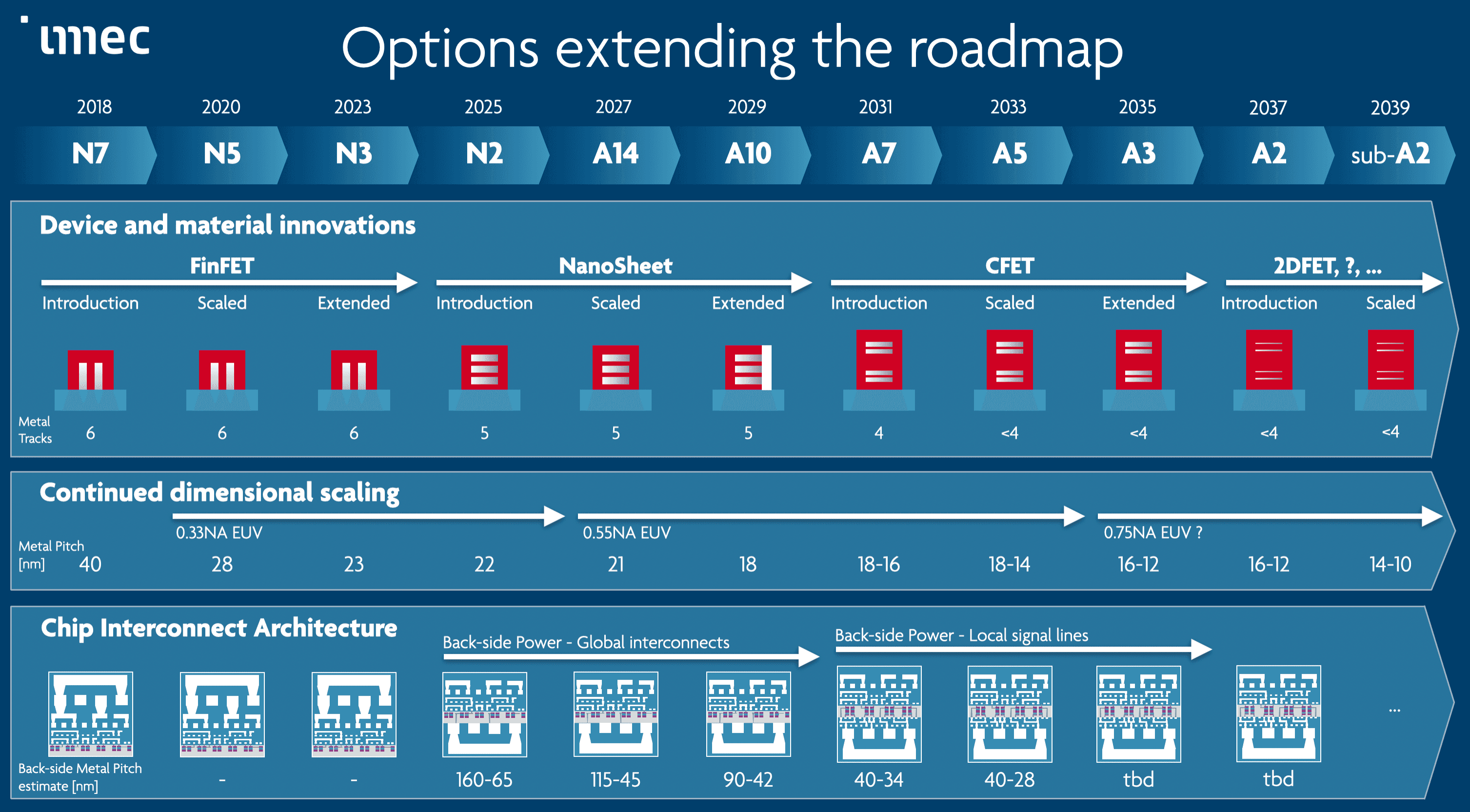
Figure 1 – The imec logic technology roadmap.
That’s where 2D semiconductors, more particularly, transition metal dichalcogenides (MX2), provide an opportunity. In these semiconductors, atoms are arranged in layered crystals with a single layer thickness of only ~0.7nm, allowing for very thin channels. In addition, they promise to maintain a relatively high carrier mobility independent of channel thickness. This enables ultimate gate and channel length scaling without worrying about short channel effects.
2D material integration in advanced nodes: challenges
The big performance leap that 2D channel materials can deliver at ultimately scaled nodes has sparked the interest of major chip manufacturers and academic leaders in the field. Encouragingly, they have started to invest heavily in research and development to overcome the obstacles of introducing 2D materials in the most advanced nodes. 2D-material integration indeed comes with its own set of challenges, adding to the cost and integration efforts towards A2 node introduction.
2D material deposition
First, there is the challenge of depositing the 2D materials layers. For applications requiring high-performance devices, two main routes can be followed: (1) direct growth of the 2D material on the target substrate, and (2) the growth on a ‘growth substrate’ followed by a transfer of the layer to the target substrate.
Direct growth of the 2D material normally requires specific substrates and occurs at high temperatures (~1000°C). If industry compatible processes and materials are required, the growth substrate may however not be ideal for inducing a high degree of crystallization – degrading the film’s performance. Nevertheless, direct growth may offer conformality, wafer level coverage and compatibility with industrial processes.
In the second approach, growth can take place on a foreign ‘ideal’ substrate (such as sapphire), facilitating high performing films and subsequent transfer to the target wafer. The transfer itself can be performed at much lower temperatures (around 300°C) than in the direct growth case. The increased number of process steps induced by transfer may however impact the cost and yield of the chip fabrication process.
Gate stack integration
A second challenge relates to gate stack integration and dielectric deposition. Ironically, the very reason why 2D materials can be made so thin is also responsible for complicating dielectric deposition. The layers that make up the 2D materials are vertically bound to each other by very weak van der Waals (vdW) forces, leaving the surface mostly passivated – without any dangling bonds. This challenges the use of deposition techniques that have worked so well on Si, including atomic layer deposition (ALD) which relies on the interaction with dangling bonds on the surface.
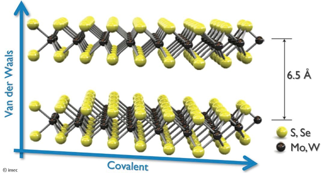
Figure 2 – Layers of 2D materials (WS2) bonded by weak van der Waals forces.
In recent years, good progress has been made by imec and leading chip manufacturers, and n-type nanosheet 2D-channels with integrated gate stacks have been demonstrated – although mainly on lab-based devices [1-6].
Low-resistance source/drain contacts
A third major challenge is the formation of low-resistance source/drain contacts. In the case of Si, source/drain contacts are formed by bringing a metal in contact with the source/drain regions, creating a Schottky barrier at the interface. Charge carriers can then be injected into the source by means of tunneling. To ensure low-resistance source/drain contacts, two key techniques are applied: (1) heavily doping of the source/drain regions; and (2) the formation of silicides. These enabling techniques are however very difficult to achieve on thin layers of 2D materials, spurring researchers to explore alternative solutions. [7-9]
Doping of 2D materials
Doping of 2D materials is not only critical for obtaining low-resistance contacts. It is also required for tuning the threshold voltage (Vth) in the channel and for reducing the access resistance. Differently to its 3D counterparts, substitutional doping in 2D materials using conventional ion beam implantation greatly degrades the transport properties of the material. Due to its extremely thin nature, replacing even one atom in the lattice is much more impactful for 2D materials than 3D materials. Other techniques for doping are being explored (such as electrostatic doping or surface doping) but there is still no clear solution.
p and n type FETs
CMOS technology applications rely on a combination of both n- and p-channel FETs. In standard CMOS technologies, Si is used to form both types of FETs. But no 2D material has been found so far to make that possible: the optimal material used for n types (such as MoS2) is not the optimal material for p-type FETs (with WSe2 being most promising).
Fab integration and the need for increased reliability and variability
Finally, until recently, research has mainly been carried out in the labs, where ‘hero’ devices could be obtained on cm-scale coupons. Huge development efforts are however needed to bring the processes to an industrial scale, compatible with 300mm wafer integration [10]. In parallel, a boost in reliability and strong reduction of the variability are needed.
Introducing 2D materials in lower performant devices – an imec approach
While leading chip manufacturers and university groups are seeking solutions for introducing 2D materials in the conduction channels of the most advanced CFET architectures, imec takes a different turn – driven by the many integration challenges and expected costs.
To reduce efforts and expected costs of introducing 2D materials, we opt to phase them into less advanced nodes and in less performing devices. We start focusing our module developments and 300mm wafer process development on planar 2D devices. By the time we need to integrate them into very complex CFET architectures, we can fall back on what we have learned. The 2D material will have already been introduced into the 300mm fab, solutions will be ready for dielectric deposition and source/drain contact formation, and routes will have been explored for increasing reliability and variability. Below, imec’s approach is described in more detail.
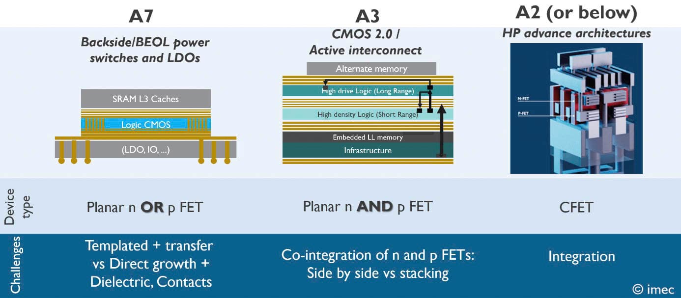
Figure 3 – Opportunities for 2D MX2 devices – an imec approach.
Planar 2D-based n or pFETs in the A7 technology node
Imec is working on introducing 2D MX2 based devices first in the A7 node of the imec logic technology roadmap. In this future technology generation, CFETs with Si channels will make up high-performant logic CMOS, power will be routed to these logic devices by BSPDNs, and last-level cache memory may connect to the logic CMOS through advanced 3D integration technologies. An opportunity for planar 2D MX2 based devices are peripheral devices, residing in the back-end-of-line (BEOL) or even in the backside of the wafers. Think about low dropout voltage regulators (LDOs) and lower performant power switches that turn on (and off) blocks of logic CMOS devices.
Simulations by imec researchers show that planar nMOS devices with MX2 channel are very promising for such applications. In the wafer backside or BEOL, there will be more space available to implement them. As such, their footprint can be relaxed compared to their (expensive) frontside counterparts, leaving room for larger, planar device architectures – either n or p type. For these applications, layer transfer is the preferred deposition technique: BEOL and backside processing both limit the available temperature budget to sub-400°C, as not to degrade the performance of the devices already present in the frontside. Direct growth of 2D materials at these low temperatures (in an industrially compatible fashion) is challenging, as it might result in layers of bad quality.
Planar 2D-based n and pFETs in the A3 node
In parallel, developments are ongoing for inserting the material in the imec A3 technology node. Here, imec anticipates the gradual transition towards CMOS 2.0 – a paradigm change that allows to unlock the potential of Moore’s Law by bringing hybrid integration inside the compute system-on-chip (SoC) [11]. It does so by re-partitioning the SoC into different functional layers (with the aid of STCO) and re-connecting them using advanced 3D interconnect and backside technologies. Instead of using the most advanced nodes for each functional part of the SoC, the functional layers can be built using the technology option that most closely matches their constraints. The layers that require extreme device density (e.g., the dense logic) will be made up of the most scaled technologies (i.e., CFET).
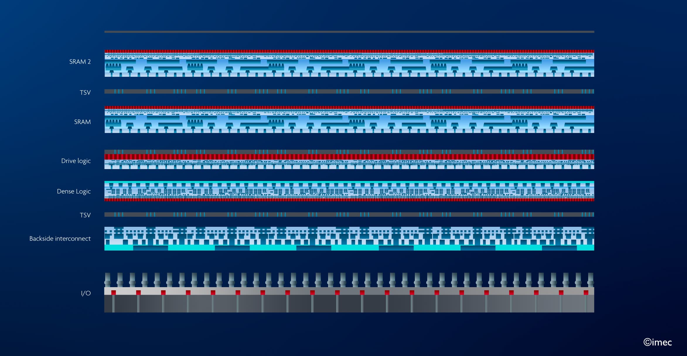
Figure 4 - Example of a possible partitioning of an SoC in the CMOS 2.0 era.
CMOS 2.0 allows a smooth introduction of 2D materials in different layers of the SoC. For example, power switches as part of the active interconnects in the wafer’s backside, or planar MX2 devices as part of the memory layers.
2D-based GAA nanosheets and CFETs
While the above developments are taking place inside the 300mm cleanroom, imec at the same time explores the introduction of 2D materials as conduction channels in GAA nanosheet transistors. These studies take place at lab scale but do use fab-compatible tools and processes. The aim of these investigations is to address the impact of 2D material integration on nanosheet-specific modules, which will be relevant to CFET on the longer term. Think about the nanosheet channel release (i.e., the removal of sacrificial layers to form the nanosheet channels), inner spacer formation and the replacement metal gate integration step.
Learnings obtained on lower-performant planar MX2 FETs: layer transfer, pFET integration and increased reliability
300mm templated growth and layer transfer: a viable route towards uniform, high-quality 2D monolayers
Templated growth and layer transfer of 2D materials is an interesting approach to deposit high-quality layers of 2D materials on 300mm target wafers at temperatures below 400°C. With templated growth, a pre-defined ‘templated’ substrate (such as sapphire) is used to direct the growth of the 2D materials into one single crystal orientation. Afterwards, the ultrathin layers spanning the entire 300mm wafer surface need to be transferred to the target wafer without breaking.
At 2024 VLSI, imec has demonstrated a 300mm MX2 dry transfer process flow which resulted for the first time in a repeatable process with excellent uniformity over the wafer (>99.5% morphological yield) [12]. In addition, the number of defects was significantly reduced compared to other layer transfer approaches. Key to obtaining these breakthrough results is the use of bond front initiation during performant bonding, and photonic debonding during release of the temporary carrier. Bond front initiation is based on first applying a bonding force at the center of the wafer, which is then propagated towards the edges. The techniques were shown to mitigate void formation, improve bonding uniformity and yield little to no residues.
Figure 5 – Imec’s 300mm MX2 dry transfer process flow, including bond front initiation and photonic debonding. On this test vehicle, Si/SiO2 was used as the MX2 growth template (as shown at 2024 VLSI).
This makes layer transfer a viable option for 2D material deposition. The proposed process flow uses 300mm compatible fabrication steps that are well-known to the chip industry – in the context of 3D SoC and chiplet integration.
Layer transfer applied on lab-based GAA nanosheets: good layer conformity and quality
The imec team has applied the learnings obtained from the layer transfer on planar devices to GAA nanosheet test vehicles. The results show lab-based MX2 nFETs with excellent conformity, uniformity and layer quality. Layer transfer is an interesting approach for nanosheet channel-formation (so, also for CFETs), which is preferably done at temperatures below 600°C.
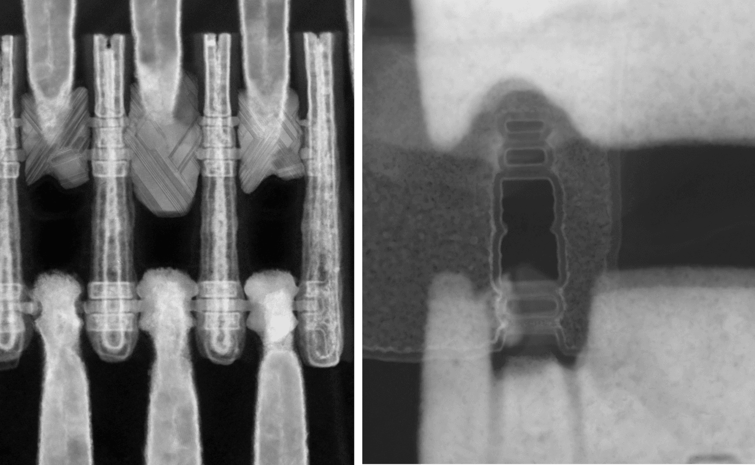
In addition, at 2024 IEDM, imec for the first time reported functional stacked nanosheet FETs with monolayer MoS2 channels deposited via layer transfer on 300mm target wafers. The device shows comparable Ion (~451µA/µm) and record on-off ratio (>109) compared to state of the art. Learnings based on planar devices were used for critical module development, including the gate module [13].
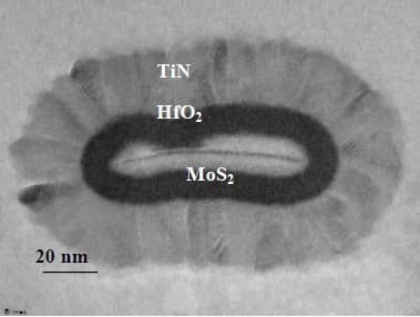
Figure 6 – TEM cross-section of a monolayer-MoS2 nanosheet FET with high-k and gate metal fully wrapped around the channel (as presented at 2024 IEDM).
Alternatively, imec explores direct growth of 2D materials at reduced temperatures, which may enable good quality layers only when deposited at smaller, selected areas.
A 300mm integration platform for 2D-based planar pFETs
So far, most integration efforts have been made on n-type devices. At IEDM 2023, imec in collaboration with Intel were the first to demonstrate 300mm integrated planar WSe2 pFET transistors, using a similar process flow as for MoS2 nFETs [14]. The teams also provided a clear analysis of the impact of grain size on the performance and reliability of the device.
A path to increased reliability and reduced variability
In previous years, imec and Vienna University of Technology (Prof. Tibor Grasser’s group) made progress in quantifying the reliability and variability of 2D-material based devices. They studied the impact of, for example, 2D layer thickness, crystal grain size and orientation, and 2D growth template on the performance of 300mm integrated MX2 planar devices. They were also able to identify the root cause of the reliability and variability issues and are now working towards solutions. [15]
Addressing the remaining challenges: a collaborative effort
While big leaps forward have been made by various research groups worldwide, some breakthroughs are still needed to bridge the gap towards high-volume manufacturing at advanced nodes. Imec identifies fab-compatible source/drain contact formation, controllable doping and the enablement of CMOS with MX2 devices (i.e., integrating p and n type FETs together) as the most critical obstacles going forward. Solving these issues requires a collaborative effort, involving industry leaders, university groups and research institutions, as well as tool developers.
With these issues solved, the future looks bright for 2D materials. Not only do they promise to advance the logic scaling roadmap from A7 on, but their characteristics also allow to expand the application domain far beyond logic. Benefiting from their extremely low off-state current, they show potential for embedded DRAM applications – possibly from the A7 node onwards. In addition, the transport properties of ‘surface-like’ 2D materials are very easy to perturbate, and this makes them ideally suited for probabilistic computing or even machine learning applications.
This article was originally published in Semiconductor Digest.
Want to know more?
[1] ‘First Demonstration of GAA Monolayer-MoS2 Nanosheet nFET with 410μA μ m ID 1V VD at 40nm gate length,’ Y. Chung et al., 2022 IEEE International Electron Devices Meeting (IEDM)
[2] ‘High Mobility TMD NMOS and PMOS Transistors and GAA Architecture for Ultimate CMOS Scaling’, A. Penumatcha et al., 2023 IEEE International Electron Devices Meeting (IEDM)
[3] ‘Status and Performance of Integration Modules Toward Scaled CMOS with Transition Metal Dichalcogenide Channel,’ A. Chou et al., 2023 IEEE International Electron Devices Meeting (IEDM)
[4] ’Monolayer-MoS2 Stacked Nanosheet Channel with C-type Metal Contact,’ Y. Chung et al., 2023 IEEE International Electron Devices Meeting (IEDM)
[5] ‘Dual gate synthetic WS2 MOSFETs with 120µS/µm Gm 2.7µF/cm2 capacitance and ambipolar channel,’ D. Lin et al., 2020 IEEE International Electron Devices Meeting (IEDM)
[6] ’Scaling synthetic WS2 dual-gate MOS devices towards sub-nm CET,’ D. Lin et al., VLSI 2021
[7] ‘Yttrium-doping-induced metallization of molybdenum disulfide for ohmic contacts in two-dimensional transistors,’ Jiang, J., Xu, L., Du, L. et al., J. Nat Electron 7, 545–556 (2024). https://doi.org/10.1038/s41928-024-01176-2
[8] ‘Antimony Semimetal Contact with Enhanced Thermal Stability for High Performance 2D Electronics,’ A. -S. Chou et al., 2021 IEEE International Electron Devices Meeting (IEDM), San Francisco, CA, USA, 2021, pp. 7.2.1-7.2.4, doi: 10.1109/IEDM19574.2021.9720608
[9] ‘Advancing 2D Monolayer CMOS Through Contact, Channel and Interface Engineering,’ K. P. O'Brien et al., 2021 IEEE International Electron Devices Meeting (IEDM), San Francisco, CA, USA, 2021, pp. 7.1.1-7.1.4, doi: 10.1109/IEDM19574.2021.9720651
[10] ‘Process integration and future outlook of 2D transistors,’ K.P. O’Brien, Nature Communications volume 14, Article number: 6400 (2023)
[11] ‘CMOS 2.0: bringing heterogeneity inside the system-on-chip’, imec Reading Room
[12] ‘EOT scaling via 300mm MX2 dry transfer – Steps toward a manufacturable process development and device integration’, S. Ghosh et al., VLSI 2024
[13] ‘High-performance monolayer-2D stacked nanosheet FETs with high ION ~ 451 μA/μm and ION/IOFF > 109’, F. Xi et al., 2024 IEEE International Electron Devices Meeting (IEDM)
[14] ‘Exploring manufacturability of novel 2D channel materials: 300mm wafer-scale 2D NMOS & PMOS using MoS2, WS2, & WSe2,’ C.J. Dorow, T. Schram et al., 2023 IEEE International Electron Devices Meeting (IEDM)
[15] ‘Evidence of contact-induced variability in industrially-fabricated highly-scaled MoS2 FETs,’ L. Panarella et al., npj 2D Materials and Applications volume 8, Article number: 44 (2024)

César Javier Lockhart De La Rosa received his B.S. degree in electronic engineering from Universidad APEC, Dominican Republic, and the M.Sc. degree in nanoscience and nanotechnology from KU Leuven, Belgium, and Chalmers University, Sweden, in 2012. After that he got his Ph.D. degree from KU Leuven in collaboration with imec, Belgium, in 2017 and Post-Doc in 2018 tackling the contacts and doping of 2D TMDCs and graphene-based transistors for logic applications. He then worked as a researcher at imec in different domains such as selector devices for memory applications and DNA for data storage before becoming the program manager for Exploratory Logic program where he drives the efforts to identify and integrate the next generation logic devices.

Gouri Sankar Kar received his Ph.D. in semiconductor device physics from the Indian Institute of Technology, Kharagpur, India, in 2002. From 2002 to 2005, he was a visiting scientist at the Max Planck Institute for Solid State Research, Stuttgart, Germany. In 2006, he joined Infineon/Qimonda in Dresden, Germany, as lead integration engineer and was responsible for vertical transistor development for the DRAM application. In 2009, he joined imec, Leuven, Belgium, where he is currently working as the VP R&D Compute & Memory Device Technologies
Published on:
16 January 2025

