The downside of a general-purpose technology platform
Julien Ryckaert: “For several decades, the advancement of monolithic systems-on-chip (SoCs) for high-performance computing (HPC) – such as CPUs and GPUs – hinged on the success of CMOS scaling. CMOS offered SoC developers a technology platform that allowed them to integrate more and more functions on one and the same substrate. Even with the evolution towards multi-core architectures, it turned out more efficient to integrate every function on a common substrate than to move data around between different chips. In addition, the SoC’s power, performance, area, and cost (PPAC) could be improved just by scaling the transistors and the interconnects from one node to another. The most scaled technology was applied in every functional part of the SoC – from computing blocks to cache memory to the infrastructure that wraps the system (including electrostatic discharge (ESD) protection devices, power and clock distribution, signal networks, and input/outputs (I/O)).
For a long time, this CMOS platform served different computational needs, for mobile applications as well as for HPC.
But this general-purpose technology platform gradually began to break, for two reasons. First, dimensional scaling started to provide diminished PPAC returns at the system level. Second, the once praised heterogeneity of the SoC – created by adding more and more functions in a 2D fashion – progressively became its own bottleneck: with only one technology at hand to build all the critical functions of the SoC, it became increasingly challenging to address the rising variety of compute specificities (in terms of power density, memory bandwidth, speed, workloads, cost, form factor etc.) that came with the increasing diversification of applications.”
CMOS 2.0: a different approach to miniaturization
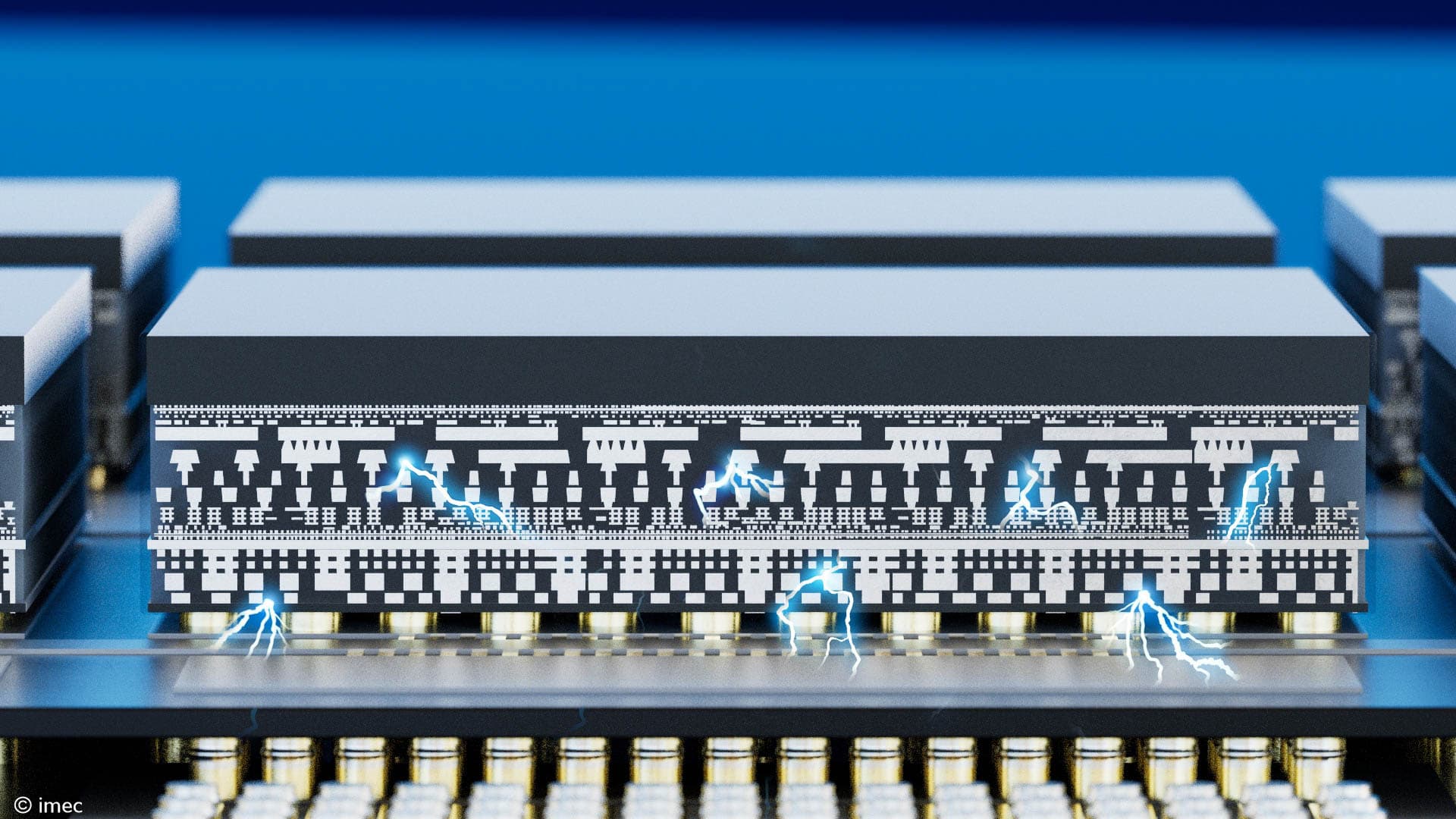
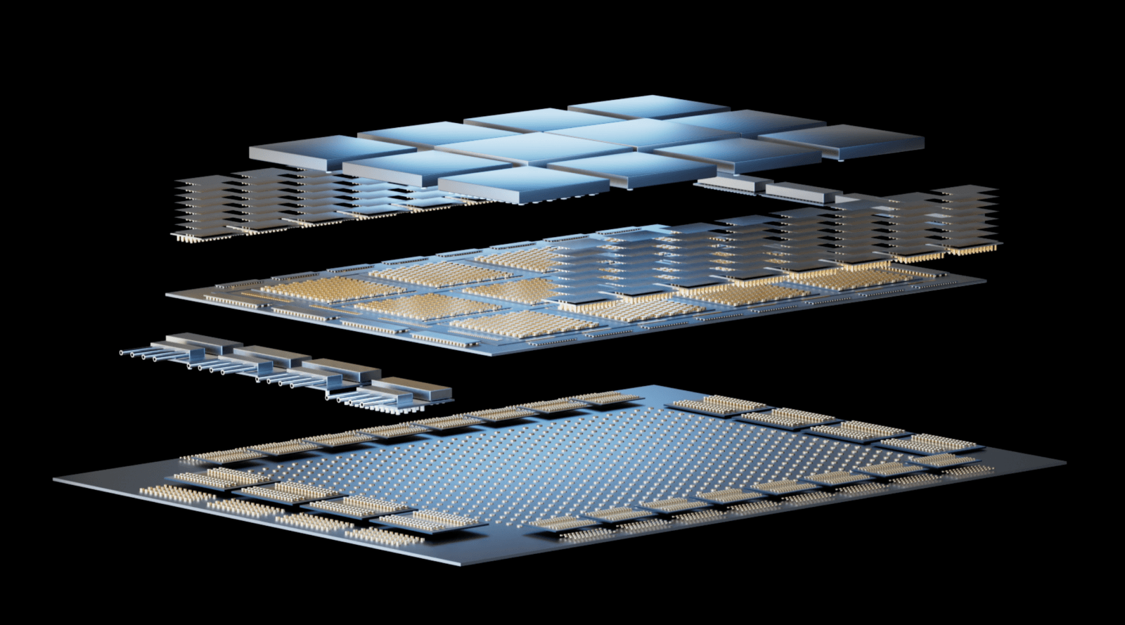
“Driven by general-purpose scaling issues, with CMOS 2.0 we approach miniaturization in a different way. Instead of using the most scaled technology for each function within the SoC, why not re-architect the whole SoC and partition it into different functional layers – with the aid of system-technology co-optimization (STCO)? Each of the layers can be built using the technology option (in terms of devices, technology nodes and interconnects) that most closely matches the constraints of that particular functionality. The most scaled technologies – enabled by the continuation of Moore’s Law – are reserved for those layers that require extreme device density.
Advanced 3D interconnect technologies then re-connect the heterogeneous tiers of the SoC with a connectivity performance as if these parts were on the same substrate. CMOS 2.0 will build upon 3D integration technologies that have already shown tremendous opportunities in assembling heterogeneous parts together. Think about the 3D stacking of an SRAM chip on top of a processor to increase memory capacity; or connecting scaled-out processing systems with an active interconnect layer. The profound evolutions in 3D interconnect technologies of the last five years and the rise of functional backside technology will allow us to bring this heterogeneity inside the SoC itself.
CMOS 2.0 is a paradigm change that allows to unlock the potential of Moore’s Law in a different way. We can now enter a roadmap with a new trajectory for CMOS scaling. We can tune CMOS scaling to the needs of the most demanding layers and lift all other constraints. In addition, breaking up the SoC into different layers and optimizing each layer separately will offer greater versatility for system optimization. New technology platforms will emerge that can address a broader range of compute applications – thereby expanding the application domain from high-performance mobile, HPC and AI/GPU towards emerging AR/VR, 6G wireless and automotive applications.”
Illustrating the CMOS 2.0 way of thinking: partitioning the SoC’s logic part
“Let’s have a look at the logic part of the SoC. In the classical, CMOS 1.0 way of thinking, the continuation of the roadmap allowed us to increase the density of transistors while maintaining their performance in terms of drive current. The transition from planar MOSFET to FinFET was a good example of how we maintained that dual constraint. By transforming the conduction channel in the form of a fin, we could reduce the transistor’s footprint. At the same time, the high drive current could be maintained by tuning the height of the fin. Today, in the nanosheet family of transistors, the duality is further preserved by finding an optimal tradeoff between sheet width and number of stacked sheets. But in the future, it will be more and more difficult to extract enough current from the logic standard cells as they become more compact and must maintain a power density limit.
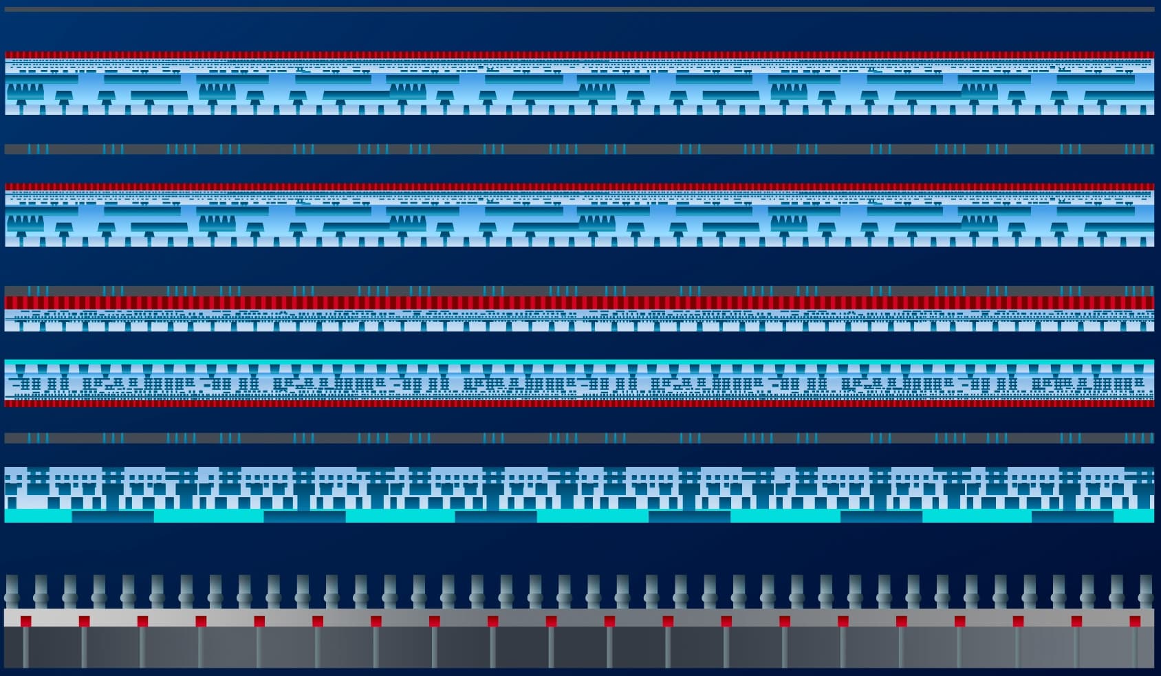
CMOS 2.0 takes a different approach. It starts from the observation that, in a design made of a billion transistors, the transistors that need to be smaller (i.e., the dense logic that connects to neighboring standard cells) are not the same as the ones that need to be highly performant (the drive logic, driving long-range interconnects). So why not split the logic part into a high-drive logic layer optimized for bandwidth and performance, and a high-density logic layer optimized for performance/Watt? The dense logic layer can be fabricated using the most advanced technologies, including advanced patterning techniques such as (multi-patterning) high-NA EUVL or even hyper-NA EUVL, and the most scaled transistor architectures such as CFET. This layer will represent most of the cost and justifies our efforts in continuing Moore’s Law. On the longer term, in this layer, we will be able to introduce new materials such as 2D materials and new beyond-CMOS logic device concepts in a smoother way, as all other constraints have been physically removed to other layers of the SoC.
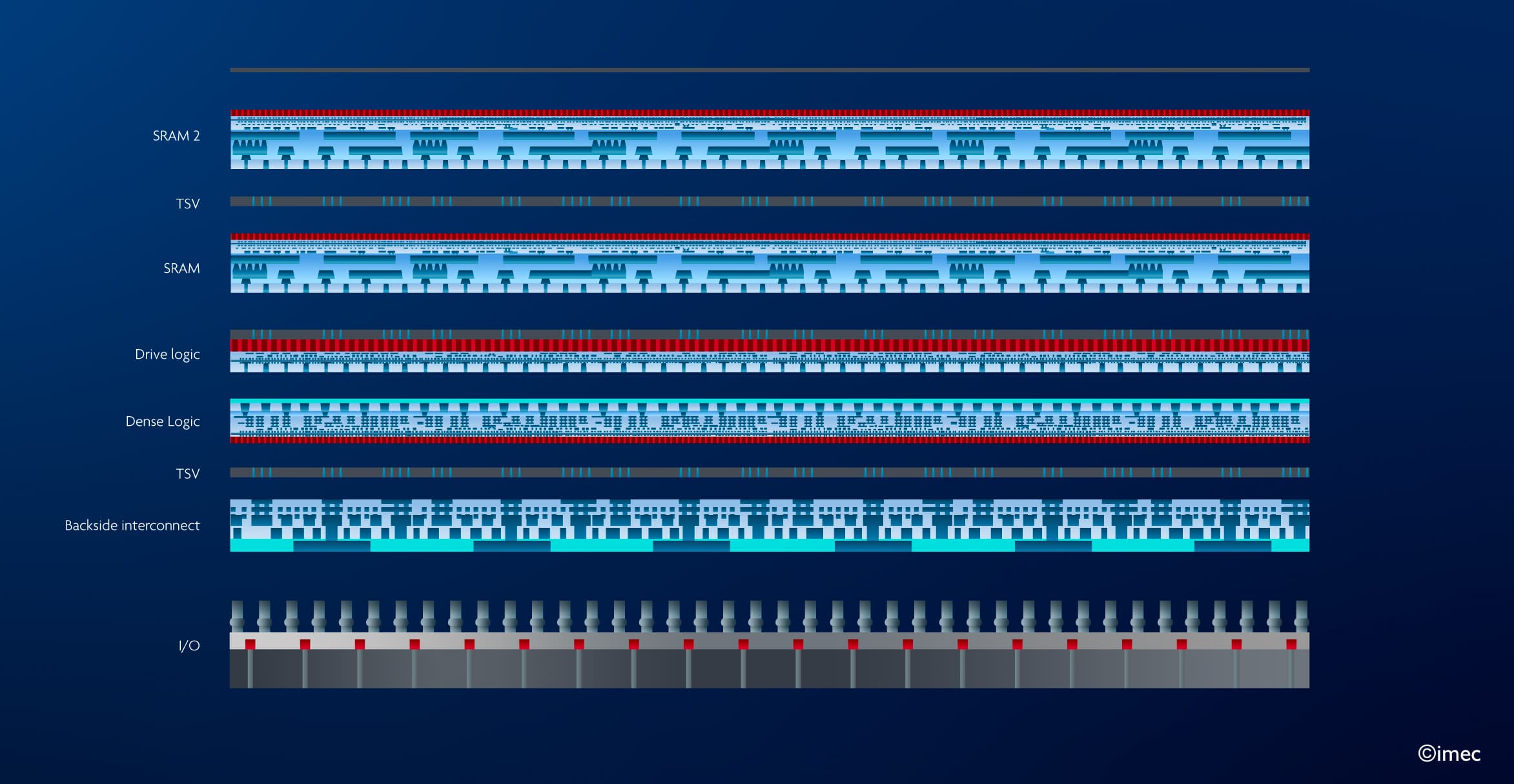
Figure 1 - Example of a possible partitioning of a SoC in the CMOS 2.0 era.
Do you want regular updates on imec’s semiconductor research?
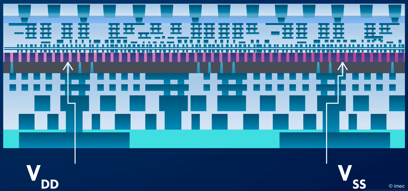
The other layers may include cache memories – leaving the option to flexibly introduce alternative embedded memory technologies in the longer term. Functionalities such as power delivery, ESD protection devices and clock signal may be contained in the SoC’s functional backside. As such, extreme BEOL pitch patterning will be possible in the frontside without the constraint of voltage drop on the power supplies. Also, devices that do not scale well, such as thick-oxide I/O, can be integrated in a separate layer. Obviously, this is just one example of a possible partitioning. In the end, the application will determine the optimal partitioning of the system, piloted by STCO.”
Key enablers: 3D interconnect and functional backside technologies
“CMOS 2.0 takes a different approach to miniaturization, but still relies on all semiconductor innovations of the past years. But it can only now become a reality thanks to recent breakthroughs in 3D interconnection technologies and the emergence of backside technologies – two critical technologies where imec and its partners are leading the way.
Profound evolutions in 3D interconnect technology can now provide layer-to-layer connectivity with the same bandwidth as in traditional monolithic planar SoC configurations. Hybrid wafer-to-wafer bonding, for example, starts to offer sub-micron interconnect pitch connectivity and, as such, enters the realm of interconnect density required for the last metal layers of the back-end-of-line. At the 2023 IEDM conference, imec demonstrated Cu/SiCN wafer-to-wafer bonding with interconnect pitches down to an unprecedented 400nm pitch. Some of the functions will need an even finer-grained disintegration, for which we will need backside technologies at the granularity of logic cells, and sequential 3D technologies at the granularity of 3D devices such as CFET. With these developments, breaking a SoC into different layers starts to become as efficient in terms of connectivity as moving data around in a monolithic SoC. On top of that, it comes with additional benefits in advancing system scaling, and in the variety of applications it can support.”
Figure 2 – TEM showing multiple Cu pads connected at 400nm pitch using hybrid wafer-to-wafer bonding
Engaging the semiconductor ecosystem
“With CMOS 2.0, scaling is entering a new era, aiming at higher flexibility and providing more options for system optimization – progressively moving from classical CMOS towards a CMOS heterogeneous platform. All the R&D we do today is already marching in that direction, think about the introduction of backside power delivery networks in industry. Bringing everything under one overarching vision – CMOS 2.0 – will allow us to push this ongoing evolution to its ultimate limits, creating more options for system scaling.
But to fully realize our vision, we need to rally the whole ecosystem to that new idea. Key to CMOS 2.0 is finding a partitioning that is most suited for the compute application for which a particular SoC is being designed. This may require rethinking established design practices and the way the system is being architected. Getting the most out of the high-drive/high-density logic split, for example, may require different compute system architectures than the ones we are used to. Today, EDA tools do not account for such changes. We need EDA and system design communities to adapt to this new reality and help us figure out the proper CMOS 2.0 partitioning we should pursue. Vice versa, we must closely engage with our design partners and inform them about the different technological capabilities, for example, which transistor we can stack on top of other ones.
Realizing CMOS 2.0 will require close collaboration and co-innovation across the entire semiconductor ecosystem. Together, we need to (re-)build the infrastructure that will drive this vision. At stake is not Moore’s Law in itself, but the ability it represents to enable economic growth and sustainable innovation.”
This article was originally published in Semiconductor Digest (pgs. 21-23).

Julien Ryckaert received an M.Sc. degree in electrical engineering from the University of Brussels (ULB), Belgium, in 2000 and a Ph.D. degree from the Vrije Universiteit Brussel (VUB) in 2007. He joined imec as a mixed-signal designer in 2000, specializing in RF transceivers, ultra-low power circuit techniques, and analog-to-digital converters. In 2010, he joined the process technology division in charge of design enablement for 3DIC technology. Since 2013, he oversees imec’s design-technology co-optimization (DTCO) platform for advanced CMOS technology nodes. In 2018, he became program director focusing on scaling beyond the 3nm technology.
Published on:
1 July 2024


