High-NA EUVL: a leap in resolution
2019 was an important milestone for extreme ultraviolet (EUV) lithography. For the first time, the EUV patterning technology was deployed for the mass production of logic chips of the 7nm technology generation. It was inserted to pattern the most critical layers of the chips’ back-end-of-line (BEOL). Thereby enabling printing metal lines with pitches as tight as 36-40nm.
2024 update: entering the High-NA EUV Lithography era
With an extremely short wavelength of 13.5nm, EUV lithography has been introduced to succeed 193nm (immersion) lithography. This transition was dictated by the Rayleigh equation for resolution. According to this equation, the resolution of a lithography tool can be improved by using light with smaller wavelength during wafer exposure. By doing this, the tool's ability to print features with a certain half pitch or critical dimension (CD) also gets better.
Moreover, the complex and expensive multiple-patterning requirements of 193nm – which involve splitting a chip pattern into two or more simpler masks – could be moved back again to single-patterning EUV.
On the development side, researchers have been continuously trying to push the single-print capability of today’s most advanced EUV full field scanner, the ASML NXE:3400B. Earlier this year, for example, imec and ASML were able to demonstrate 28nm-pitch single-exposure patterning readiness for lines/spaces. This corresponds to critical BEOL metal layers of a 5nm logic technology node. And brings the current scanner close to its resolution limit for high-volume manufacturing, which is around 13nm (26nm pitch).
Along with the evolution in logic, memory manufacturers are increasingly looking at using EUV lithography. They're looking to meet the high-density requirements for future memories. For example for patterning critical DRAM structures.
At the same time, multiple-patterning EUV lithography options are being explored to advance EUV to the next nodes. These ‘tricks’ offer more relaxed pitches. But they also come with a downside: an increased number of processing steps. These add to the cost, complexity and processing time of the patterning step.
2023 will mark a new milestone in the evolution of EUV lithography. By then, the first new generation of EUV lithography tools is expected to enter the scene. A high-NA EUV lithography scanner is projected to print the most critical features of 2nm (and beyond) logic chips in a smaller number of patterning steps.
The transition towards high-NA lithography is again justified by the Rayleigh equation. This provides a second knob for improving the resolution: increasing the numerical aperture (NA) of the projection lens. The NA controls the amount of light (more precisely, the number of diffraction orders) that is used to form the image. Which means it also determines the quality of the image.
Transitioning to higher NA imaging equipment has been applied before. Remember the move from 193nm dry to 193nm immersion lithography. At that time, the optical trick of replacing the air between lens and wafer with water allowed a 45% increase in NA.
In the case of EUV, ASML will move from the current 0.33 to 0.55NA (i.e., a 67% increase in NA). This will be achieved by redesigning the optics within the lithography system. 0.55NA EUV lithography promises to ultimately enable 8nm resolution. This corresponds to printing lines/spaces of 16nm pitch in one single exposure.
An ambitious timeline...
0.55NA EUV lithography will push the patterning towards features smaller than what is possible with current 0.33NA EUV lithography systems. But the road forward is ambitious. The development of EUV lithography systems goes back to the 2000s. And there's a ten-year time span between the installation of the first pre-production EUV scanners and the recent introduction of EUV lithography in high-volume manufacturing.
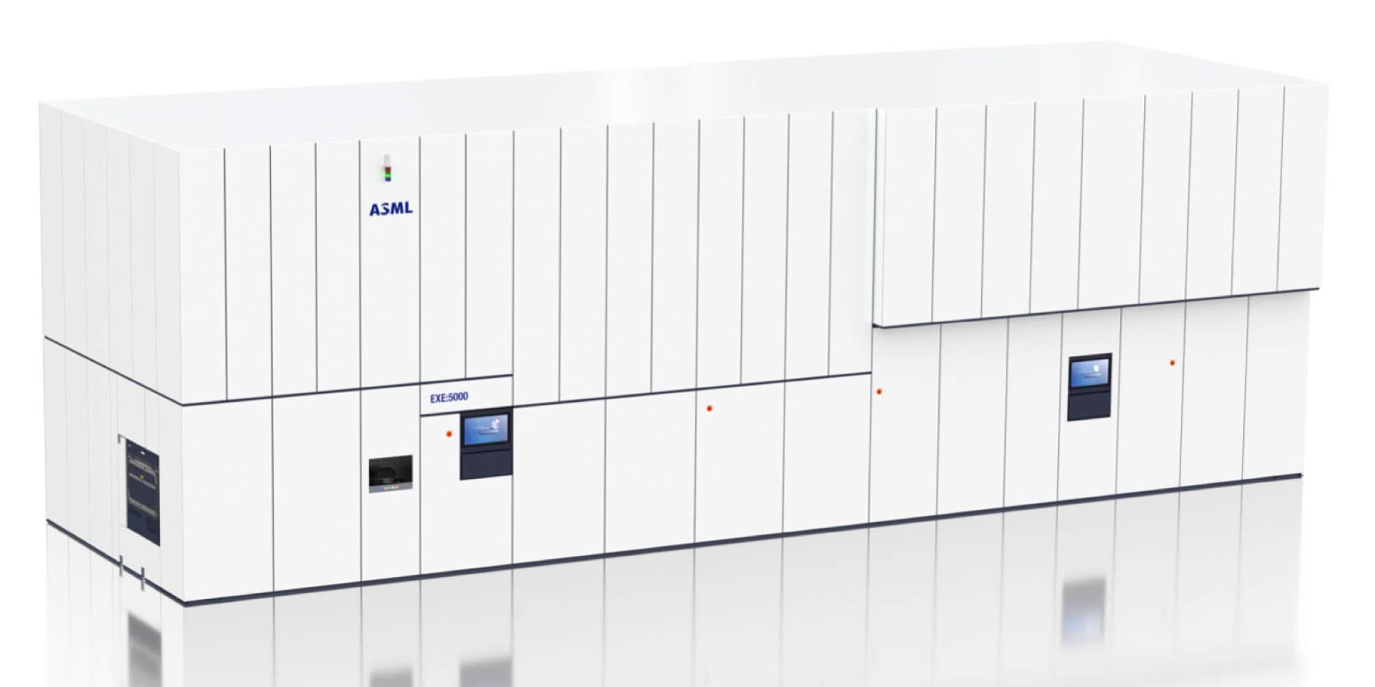
For high-NA, the ambition is to compress that time frame to only 3 years. A first prototype (the EXE:5000) is foreseen for 2023.
Do you want regular updates on imec’s semiconductor research?
Figure 1: Rendering of ASML’s EXE:5000 high-NA EUV lithography scanner (courtesy of ASML).
Prior to the availability of the first high-NA tool, dedicated lab equipment and current-generation EUV lithography tools and materials are being pushed to their extreme limits. This is necessary to prepare and de-risk the new high-NA EUV lithography technology as much as possible.
Simultaneously, imec is partnering with ASML to open a joint High-NA Lab. Here, the high-NA systems will be built, linked to a coat and development track and surrounded with metrology equipment.
Together, ASML and imec will create the ecosystem for the industry to meet the process requirements and establish the infrastructure that go along with high-NA tool development. This includes anamorphic imaging, new mask technology, metrology, resist screening and materials development for thin film patterning. These developments are discussed in more detail below. In addition, customers will have access to the High-NA Lab to develop their private high-NA use cases.
The high-NA ecosystem is ramping up
Addressing high-NA EUVL process and metrology needs: a joint effort
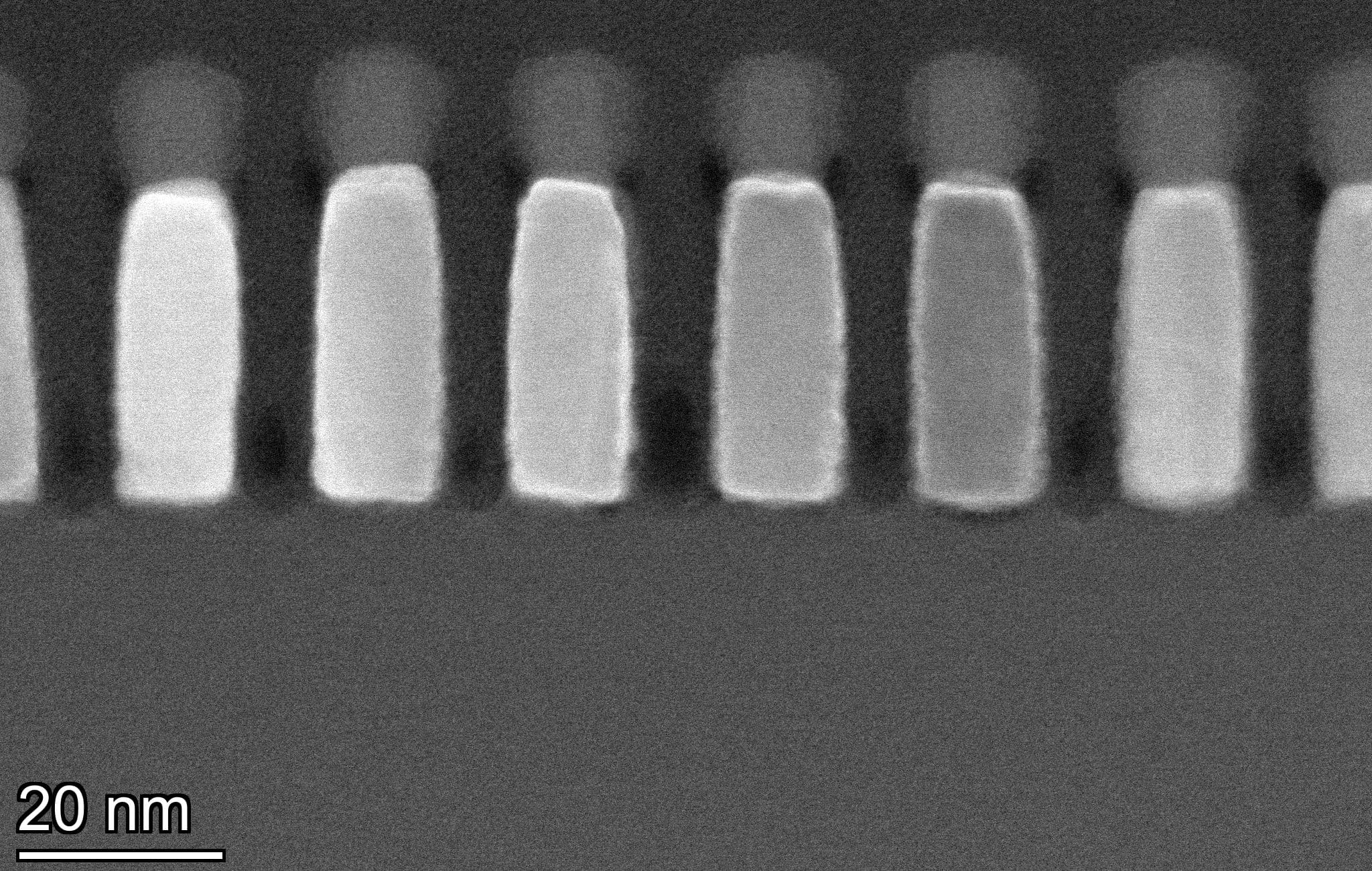
The tendency towards thinner resists will continue with the advent of high-NA EUV lithography. This ultimately aims at printing lines/spaces of 16nm pitch, corresponding to printing lines with widths as small as 8nm. This calls for resist films thinner than 20nm to maintain the ideal aspect ratio of 2:1 (defined as the ratio between the height and the width of the line). With thicker resists, the aspect ratio would increase, and with it the risk of line collapse.
High-NA EUV lithography brings a second reason for using thinner resist films. Following a second Rayleigh equation, the depth-of-focus (DOF) – i.e., the resist height across which the (aerial) image is in focus – decreases by the square of the numerical aperture. Simulations predict an effective decrease of DOF with a factor of 2-3 with respect to current 0.33NA lithography. A transition from thicker to thinner resists is therefore needed to cope with both a lower DOF in high-NA EUV lithography and a reasonable aspect ratio.
The reduced resist thickness requirements bring new needs for the high-NA EUV processes, including patterning transfer. There's a major role for imec, in collaboration with its material suppliers. They will need to screen (new) resists, optimize hard masks and select etch processes, and assess the patterning limits when going to ultrathin resists.
But the transition to smaller features and thinner resist films also challenges the metrology. More than ever, there is a strong need to address patterning and metrology opportunities together. The one serving the needs of the other.
For example, when the resist becomes ultrathin, the amount of material within a printed line becomes so small that it can hardly be ‘seen’ with the currently used metrology tools. For the widely used CD-SEM, for example, using thinner resists translates into a strongly reduced image contrast.
Recent experiments revealed that the type of underlayer (i.e., the layer underneath the photoresist film) can positively affect the SEM imaging contrast. But using a different underlayer to improve the metrology will in turn impact pattern transfer. And that calls for optimized etch processes. To continue optimizing pattern transfer, improved metrology tools or optimized tool settings will be needed to reliably image the patterns.
Figure 2: Evolution of the reduction in resist film thickness (HP = half pitch).
Below, we present some recent insights in both patterning and metrology.
Assessing the limits of pattern transfer
Imec uses the NXE:3400B to predict the performance of thinner resists – for both lines/spaces and contact holes. This is currently most advanced 0.33NA EUV lithography system, in anticipation of the first high-NA EUV prototyping system. Imec and ASML were able to print the smallest pitch possible with this scanner: 24nm pitch lines/spaces and 28nm pitch contact holes. This allows for the early material development required for the high-NA EUV lithography scanners.
By using this tool, the team showed, for example, that the line-edge and line-width roughness (LER/LWR) tend to increase when using thinner resist films. LER/LWR are among the most critical parameters for patterning lines/spaces. In these experiments, chemically amplified resists (CARs) were used. This is a type of resist that relies on chemical amplification of electrons formed within the resist when EUV photons hit the surface.
These CARs have been intensely used in industry since the early 1990s and have been gradually optimized for better resist performance. But for high-NA lithography, the industry might need resists beyond CARs, with better resolving power. We therefore see an emergence of novel photoresist materials such as metal oxide resists (MORs).
Our first experiments seem to indicate that these MORs have indeed a better pattern transfer capability for smaller features and thinner resists. Imec collaborates with multiple materials suppliers to develop these concepts and assess critical issues, such as contamination risks and process integration challenges.
Figure 3: Scaling down the EUV resist film thickness is observed to increase line-width roughness (LWR).
High-NA EUVL: an opportunity for metrology
As explained before, a first major challenge for metrology is the need to cope with the decreasing image contrast of presently used CD-SEM tools. Imec sees two ways to address this issue, and to continue measuring very small lines printed with ever thinner resists.
A first approach is to tweak the tool’s settings. Playing with some of the knobs of the CD-SEM tool (such as the scan rate) turns out to positively affect the imaging contrast. This makes patterns visible even at film thicknesses down to 15nm.
A second approach is to explore alternative metrology techniques, in close collaboration with imec’s metrology suppliers. Very promising in terms of resolution are low-voltage SEM, helium ion microscopy, scatterometry, ...
Figure 4: Reducing the resist film thickness (from 30nm to 10nm) (top) negatively affects the CD SEM image contrast. But (middle) can be improved by playing with CD-SEM metrology knobs or (bottom) by using different underlayers.
Apart from lines of e.g. 10nm width, there are even smaller features within the pattern that need to be imaged. As scaling continues, it has become more difficult to measure parameters like LER and overlay performance (i.e., how well one layer is aligned with the next one). This requires an image resolution far below 10nm.
And then there is defectivity. More particularly, the appearance of stochastic print failures: random, non-repeating, isolated defects such as microbridges, locally broken lines and missing or merging contacts.
They are believed to arise from the fundamental relationship between energy and wavelength. With the wavelength getting shorter – EUV lithography operates at 13.5nm – the energy from the light source is distributed over less photons. Consequently, there are just a few photons to create a pattern.
Besides this so-called “photon shot-noise effect”, stochastic effects originate from the molecular nature of matter, and the probabilistic behavior of their interactions.
The advent of high-NA EUV lithography with further increasing resolution and reduced resist thicknesses will further drive this evolution. Imec has been developing methodologies to systematically quantify the defect levels in the EUV materials and learn about the many factors contributing to the failures.
Key is the development and improvement in wafer inspection strategies which traditionally rely on optical techniques. More recently, e-beam-based inspection is gaining attention. It looks very promising for finding small defects. But it comes with a major drawback: a dramatic increase of the time needed for inspecting the full wafer. This calls for solutions for enhanced tool productivity and throughput.
Besides, electrical tests of metallized patterns are increasingly being set up to look for correlations with data obtained with optical and e-beam inspection techniques. This allows to increase learnings on stochastic patterning failures and to gain more insights into the way they impact yield.
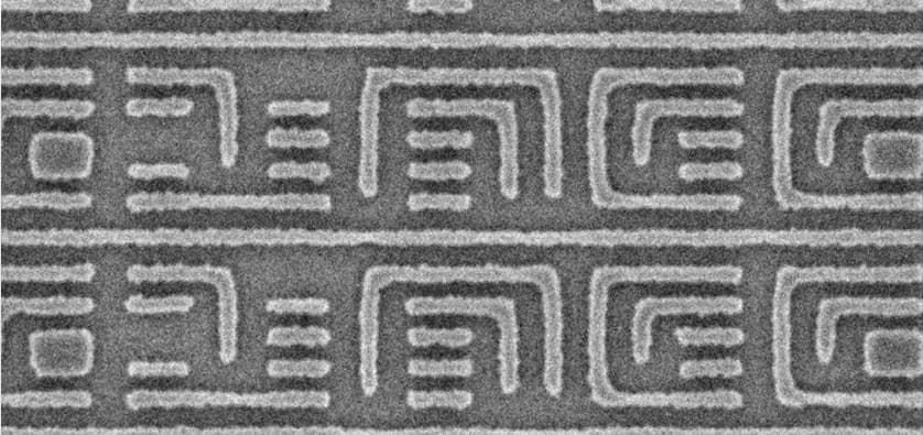
In this way, defectivity inspection data obtained with scanning electron microscopy, broadband plasma optical and e-beam technologies could already be successfully correlated with data obtained from electrical measurements. The electrical tests were carried out on large-area ruthenium-metallized serpentine structures. These allowed to measure electrical opens (and hence bridges in the resist).
The tests were also executed on metallized fork-fork and tip-to-tip structures. That allowed to measure electrical shorts (and hence critical breaks in the resist). The complementary electrical measurements showed a good correlation. And they made it possible to capture important trends across multiple process changes. That can help to mitigate stochastic printing failures.
Mask technology: another key enabler to fully exploit high-NA EUV lithography
The photomask is an essential component for the manufacturing of chips. It holds the design layout information intended for the final device. Ideally, this information is contained in dark (i.e., absorbing) and bright (i.e., reflecting) areas on the mask.
Now that progressively smaller features are being printed, deviations from the ideal mask are increasingly impacting the final wafer pattern. Mask-specific challenges therefore need to be addressed. These include, amongst others, a reduction of the mask 3D effects, an enhanced understanding of the mask lifetime and of its contribution to printing stochastic failures. The introduction of anamorphicity within the high-NA EUVL optical system brings along additional complexities to the mask industry.
In all this, the imec team has an important role to play. In close collaboration with ASML and with its material suppliers, imec contributes to the design optimization and qualification of photomasks intended for high-NA EUV lithography. This work is described in more detail below.
New absorber materials for reduced mask 3D effects
Today’s EUV masks consist of a ~300nm-thick reflective multilayer stack. This is formed by 40 to 50 alternating layers of silicon (Si) and molybdenum (Mo), capped with a thin ruthenium layer. On this stack, the absorber made of tantalum-boron-nitrate (TaBN) carries the pattern.
While the multilayer of Mo and Si reflects the incident light, the absorber blocks the reflection. This combination defines the features on the wafer.
Figure 5: Cartoon cross-section of an EUV photomask.
Current Ta-based absorbers are typically about 60-70nm thick. They're designed to absorb a sufficient amount of light. This thickness is large compared to the 13.5nm exposure wavelength of the light. Consequently, light that hits the mask under a certain angle of incidence (centered around 6° in conventional EUV lithography) and reflects from the multilayer is sensitive to the 3D topography of the ‘thick’ mask. For example, it can undergo multilayer- and absorber-induced phase deformations. This distorts the aerial image – the pattern of light that finally is transferred in the photoresist – and reduces its image contrast.
These so-called mask 3D effects also come with increased feature-dependent variations in placement and best focus on the wafer. This presents additional challenges for high-NA EUV lithography, that already suffers from a reduced DOF budget.
Originally, innovations in source illumination and mask design were applied to compensate for the mask 3D effects. In recent years, attention is shifting towards improving the mask material as the parameter to control mask 3D effects on the wafer and thus help to increase high-NA DOF.
This has driven imec’s research into exploring new absorber materials. These can have have a different EUV refractive index (low-n materials such as RuTa or PtMo allowing for attenuated phase shifting). Or a high EUV extinction coefficient (high-k materials such as PtTe or Ni with high absorbing capability).
For each of the material types, thickness optimization is required to give the best imaging trade-off. Imec is performing a material down-selection to find the most promising of these materials. New mask architectures based on these materials are expected by end of the year. They will be tested on the current EUV scanners at imec.
Figure 6: EUV mask absorber material space vs. reference TaBN.
Here comes the anamorphic mask
High-NA EUV lithography comes with a significant redesign of the optics within the scanner, allowing light with larger angles of incidence to hit the wafer – giving the system a higher resolution. At equal scanner magnification, this would come with a drawback. Light with higher angles of incidence will hit the mask as well. Without action, this would dramatically worsen the 3D mask effects.
One approach to overcome these additional shadowing effects would be to increase the mask magnification from its historical 4x to 8x, in combination with using larger mask blanks. But abandoning the original 6-inch x 6-inch mask dimensions while preserving a high mask quality would dramatically impact the mask industry. To minimize that impact, ASML and Zeiss have introduced the anamorphic lens, a lens with different magnification in the x and y directions (4x and 8y (y being the scanning direction), respectively).
The 6-inch mask is preserved, but its design is stretched in one direction. The increased magnification (in one direction) cuts the image field size (i.e., the part of the wafer that is exposed in one step) to one half. So the scanner may end up printing the features on only part of the device. This is especially true for chips with larger die sizes, imposing a constraint on how these chips need to be designed.
For these chips, chipmakers must resort to a technique called stitching. One part of the pattern is exposed with one mask, the next part with a second mask, and the two masks are stitched together. Imec investigates methods for improved stitching. One example is by reducing the so-called transition zone that inherently exists between both masks.
On the hardware side, ASML has worked towards accelerated mask and wafer stages to compensate for the loss of productivity caused by the half field imaging.
Figure 7: Schematic representation of the mask, and main orientations of mask and wafer during printing on a 0.55NA scanner (courtesy of ASML).
Pellicle development
In lithography, the photomask is usually mentioned in the same breath with the pellicle.This is the membrane used to protect the mask from contamination during high-volume semiconductor manufacturing. It is mounted a few millimeters above the surface of the photomask. If particles land on the pellicle, they will be too far out of focus to print.
Developing an EUV pellicle is not straightforward. A major challenge generic to all EUV scanners is to make the pellicle absorb as little as possible to maintain the throughput and economics of EUV lithography. In addition, the pellicle must be able to survive exposure to the increasing EUV power of future lithography tools. That includes the high-NA EUV lithography tools – for which the 8x magnification comes with the benefit of reduced power density on pellicle and mask level.
Imec, in collaboration with its partners, has developed an innovative CNT-based pellicle solution that has the potential to survive scanner powers beyond 600Watt. The CNT pellicle feasibility was already successfully demonstrated through use on the EUV NXE:3300 scanner at imec.
The team is now working to extend the lifetime. This would enable a high-productivity pellicle solution suitable for next-generation EUV lithography tools. That includes high-NA, with its strongly increased reticle acceleration.
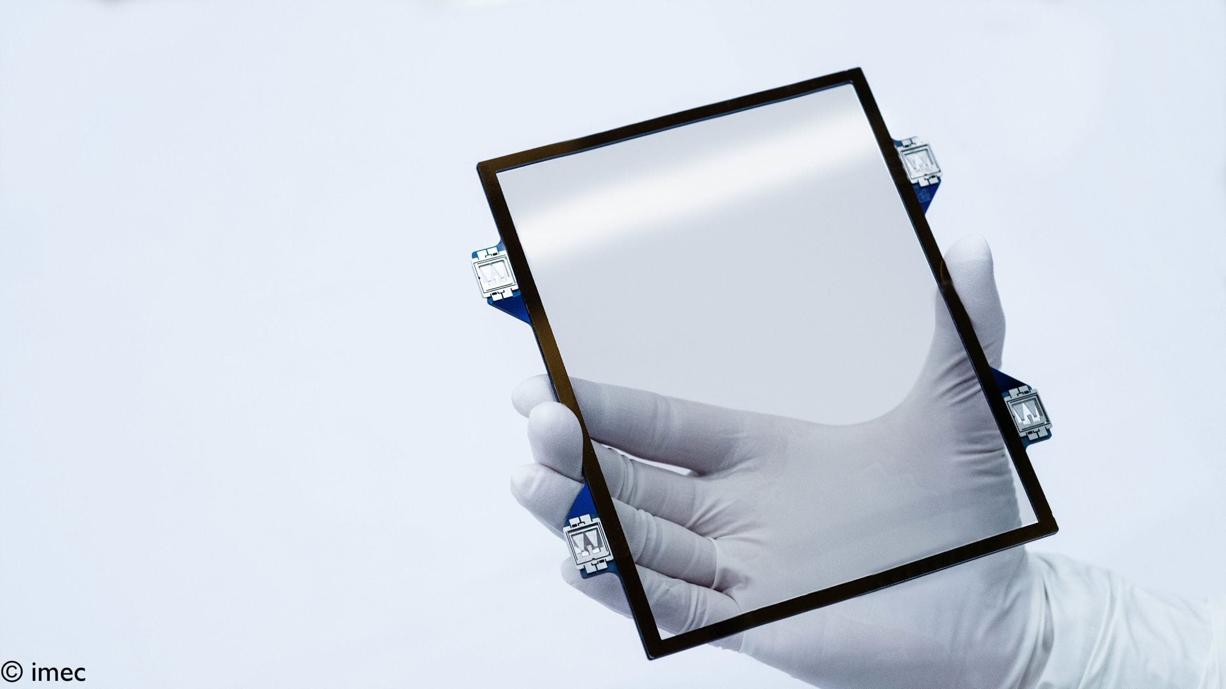
Figure 8: A full-sized CNT-based pellicle similar to those exposed in imec’s NXE:3300B
From commodity to critical component ...
The team focuses on other mask-specific opportunities, such as mask lifetime understanding. Masks are subject to carbon growth when stored. This affects the critical dimension of features printed on the wafer. The effect is observed to depend on the storage conditions and can be reversed by EUV exposure. The study revealed the importance of controlling and minimizing storage and lifetime effects as much as possible to enable stable mask printing performance.
Another challenge relates to the increasing contribution of mask deficiencies to the stochastic failure probability. The surface roughening of the mask’s multilayer, which increases with mask ageing, is observed to play a crucial role. This drives the research of alternative multilayer ‘mirror’ materials.
In addition, more than before, small imperfections on the mask such as edge placement errors or CD errors translate into errors observed after wafer printing. This has worsened now that the budgets on wafer in terms of overlay, focus and edge placement error have become extremely small, a direct consequence of scaling. And this urges the need for massively quantifying the mask contribution to the wafer imaging performance.
In addition, other methods for writing the masks with more precision and smaller resolution are being investigated. This includes multibeam mask writing, which allows for different (so-called curvilinear) mask shapes.
All this illustrates that the mask is evolving from a ‘simple’ commodity into a complex component that is becoming more and more critical to the wafer imaging performance.
AttoLab: accelerating the development of the high-NA patterning ecosystem
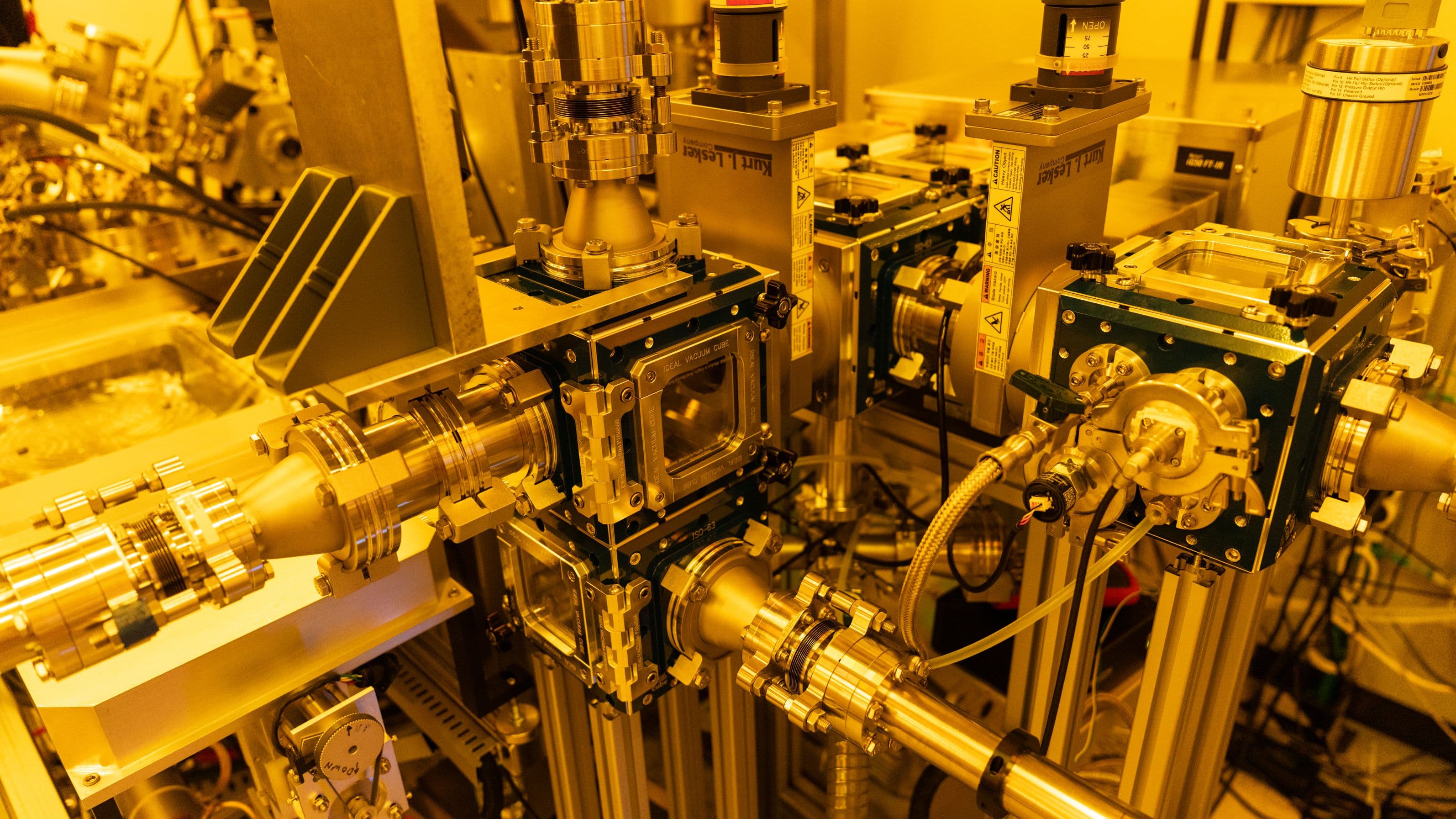
The need for speeding up learnings on thin-resist imaging was one of the reasons why imec decided to invest in AttoLab, a joint project with KMLabs. The lab allows us to explore the fundamental dynamics of photoresist imaging under high-NA EUV lithography conditions before the first 0.55NA EXE:5000 prototype from ASML becomes available. The experimental set-up offers corresponding insights on top of what is already gained from the 0.33NA EUV lithography scanners.
Within the AttoLab, the high-NA exposure at 13.5nm is emulated with a bright, coherent, high-harmonic EUV source in an interference-type of setup. Recently, with a Lloyd’s-Mirror-based interference setup for coupon experiments, 20nm pitch lines/spaces could for the first time be successfully imaged at imec in a metal-oxide resist.
In this arrangement, light reflected from a mirror interferes with light directly emitted by the 13.5nm high harmonic generation source. This generates a finely detailed interference pattern suited for resist imaging. The pitch of the imaged resist pattern can be tuned by changing the angle between the interfering light beams.
This Lloyd’s-Mirror-setup supplies the critical learnings for the next step: expansion to a 300mm wafer interference exposure (currently under installation). This can theoretically go down to an unprecedented 8nm pitch.
An interference-based type of an EUV source differs from the approach used in ASML’s high-NA EUV lasers. These vaporize tin droplets to produce EUV light. The photons subsequently bounce off several mirrors within the scanner, reflect off the mask and finally hit the resist on the wafer.
While ASML’s scanners are designed for mass production of chips, the interference type of tools as used in the AttoLab will never achieve the required full field throughput. But with these 13.5nm femtosecond enveloped attosecond laser pulses, imec is pursuing a different goal. We want to study EUV photon absorption and ultrafast radiative processes that are subsequently induced in the photoresist material. And learn more about the critical stochastic print failures.
For these studies, the beamlines are coupled with spectroscopy techniques such as time-resolved infrared and photoelectron spectroscopy. Corresponding pump-probe type of experiments are also being set up. The beamlines are designed for screening various resist materials under high-NA conditions within a few seconds. They also support the development of optimized pattern, etch and metrology technologies viable for high-NA EUV lithography.
Figure 9: Schematic representation (not to scale) of (left) Lloyd’s Mirror setup for high-NA EUV interference coupon experiments; (right) interference chamber for full 300mm wafer experiments.
Conclusion
The move from 0.33NA to 0.55 high-NA EUV lithography presents a major opportunity for the lithography community. It can jointly tackle the challenges and prepare for the tool’s introduction in a very short time frame.
Together with ASML in a joint High-NA EUV Lab, imec is focusing on the infrastructure preparation that comes along with high-NA scanner development. For that purpose, imec is relying on and invites all material and equipment suppliers to contribute to the establishment of a complete high-NA ecosystem.
The reward for all these efforts will be big. The 0.55NA EUV lithography tool promises to advance Moore’s Law towards 2nm and beyond technology generations.
Acknowledgements
This work is the result of the collaborative effort of the imec advanced patterning team, in close collaboration with imec’s equipment and material suppliers.
Want to know more?
- ‘A view on the next generation pattern technologies and materials’, imec reading room;
- ‘Imec to install high NA EUV imaging and attosecond analytical lab to probe lithography down to 8nm pitch’, imec press release;
- ‘Imec pushes single-exposure patterning capability of 0.33NA EUVL to its extreme limits’, imec press release;
- ‘Imec demonstrates 24nm pitch lines with single exposure EUV lithography on ASML’s NXE:3400B scanner’, imec press release;
- ‘Imec demonstrates 20nm pitch line/space resist imaging with High-NA EUV interference lithography’, imec press release;
- ‘Tokyo Electron to collaborate with imec-ASML Joint High NA EUV Research Laboratory’, press release.

Danilo De Simone is scientific director at imec. He has 25 years of experience in the semiconductor R&D field, and his work has produced over 100 scientific and technical papers in the field of lithographic materials and advanced patterning. Before imec, he worked for STMicroelectronics, Numonyx, and Micron Technology. De Simone is editorial board member of the Journal of Micro/Nanopatterning, Materials, and Metrology (JM3), member of SPIE committee for the Patterning Materials and Processes program and member of the International Advisory Board of the Photopolymer Science and Technology Conference (ICPST).

Gian F. Lorusso received his PhD in solid state physics from the University of Bari, Italy, in 1992. He has been working on topics related to the semiconductor industry such as metrology tool development, lithography, material analysis and more. His domains of expertise include lithography, metrology, microscopy, and spectrometry. He worked at the École Polytechnique Fédérale de Lausanne (Switzerland), the Center for X-ray Lithography (Wisconsin), the Center for X-ray Optics at Lawrence Berkeley National Laboratories (California), and KLA-Tencor (California). He joined imec (Belgium) in 2006. His work has produced more than 200 papers and 15 patents. He is working on Extreme Ultraviolet Lithography and Metrology, fields in which he started in the early nineties.

Vicky Philipsen received her PhD degree in solid-state physics from the University of Leuven (Belgium) in 2001. At imec she joined the Advanced Patterning department, where her research domain involves the study of mask 3D imaging effects in lithography (from 193nm to EUV and high NA EUV) both by simulations and experiments. She is leading the project on novel EUV mask absorbers at imec, including the technical task responsibility in European projects. She is team leader of 7 imaging researchers in the imec Advanced Patterning department and guides one PhD student.
Kurt Ronse, PhD has been working in the field of lithography at imec for almost 30 years. His responsibilities ranged from lithography researcher, lithography group manager, and advanced patterning department director to advanced lithography program director. Currently Ronse is leading the Advanced Patterning Program. That focuses primarily on the insertion of EUV lithography into HVM and on the extendibility of EUVL to the next technology nodes. Over 30 companies worldwide participate in it: chip manufactures, equipment and material suppliers, EDA/software companies, etc. Prior to joining imec, Ronse received a MS and PhD degree in Electrical Engineering from the University of Leuven (Belgium). He has authored and co-authored numerous publications and is a frequent conference speaker. He often presents invited and plenary papers, in the field of optical lithography (I-line, deep-UV, 157nm, 193nm, 193nm immersion) and EUVL. He is a member of advisory groups of various lithography conferences and has chaired several lithography conferences. He is a member of the editorial board of the SPIE Journal of Micro/Nanolithography, MEMS and MOEMS (JM3). In 2016, he has been elected Fellow of SPIE for achievements in microlithography and advanced patterning.
Published on:
4 October 2021

