What will the next two to five years bring in your area of expertise?
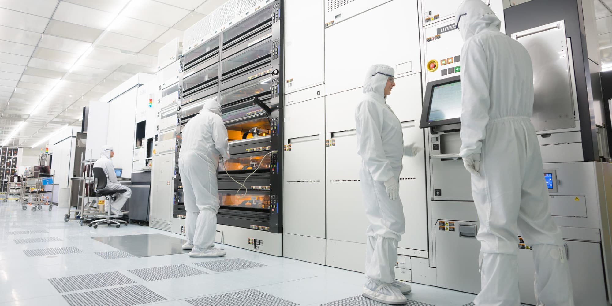
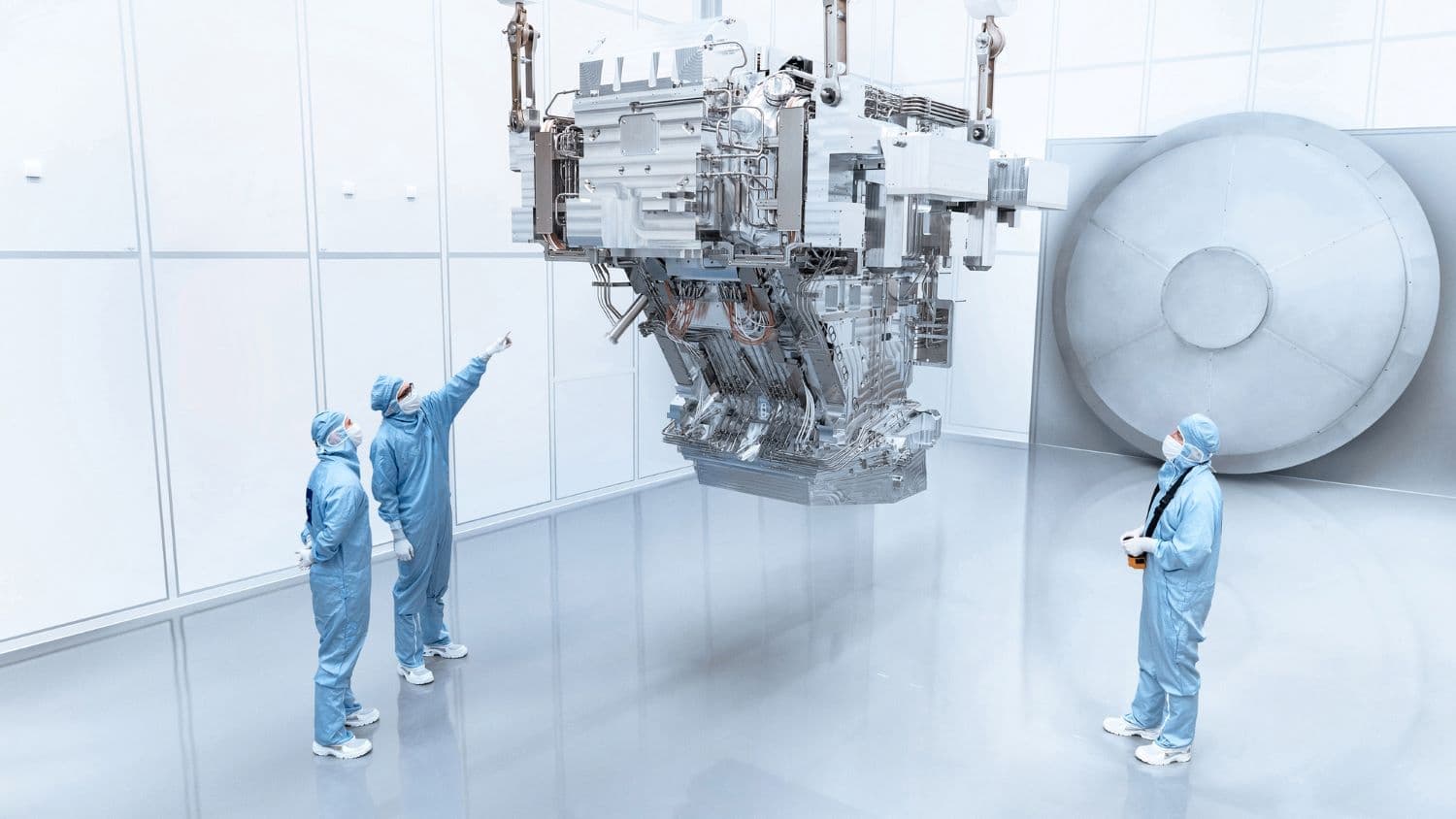
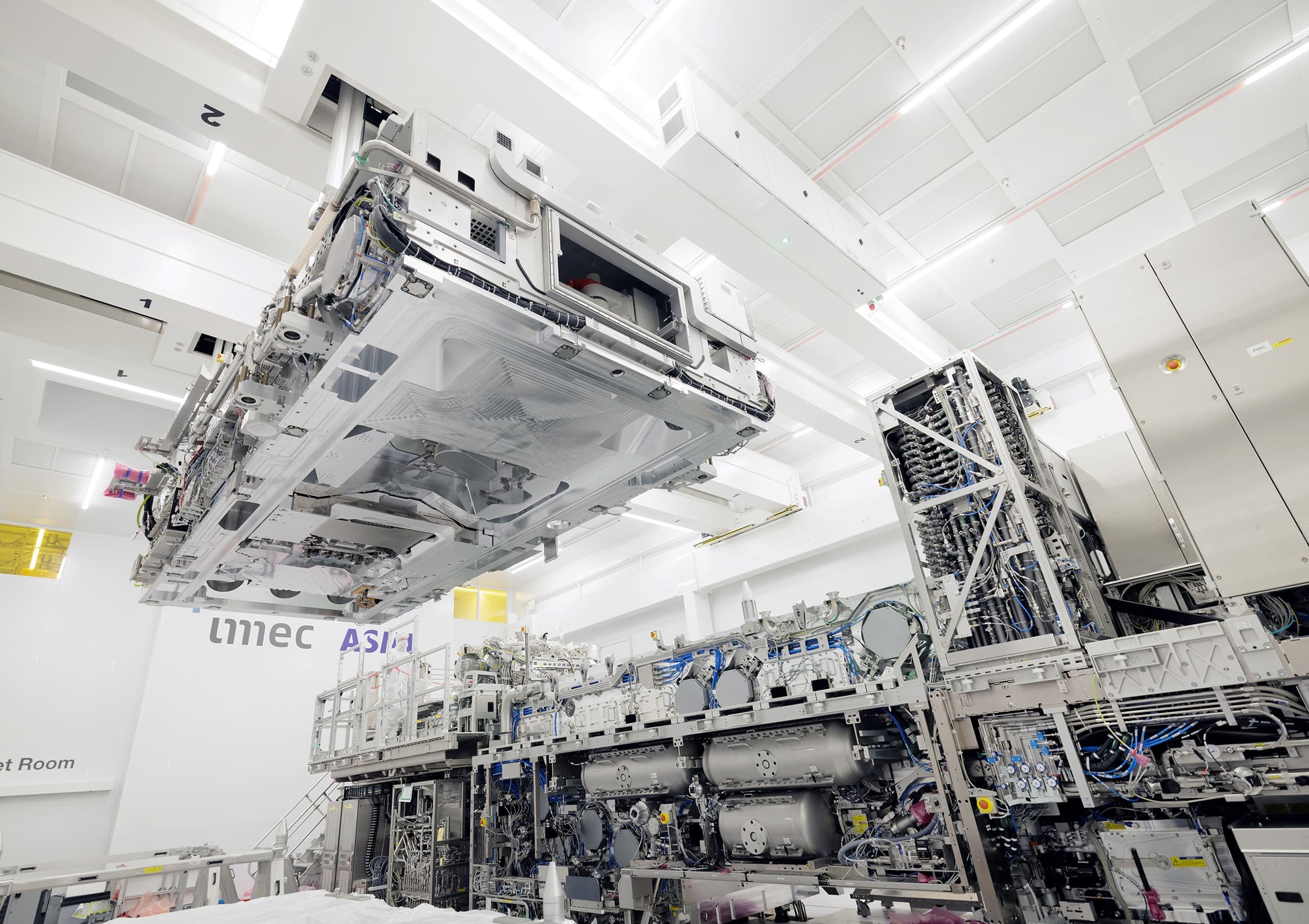
Steven Scheer: “In the course of 2025, we expect to see the introduction of the first high-numerical aperture (high-NA) extreme ultraviolet (EUV) lithography equipment in high-volume manufacturing environments. Having an NA of 0.55, these next-generation lithography tools will offer improved resolution, pushing the patterning towards features smaller than what is possible with current 0.33NA EUV lithography systems. But the road forward is ambitious. The development of EUV lithography systems goes back to the 2000s, with a ten-year time span between the installation of the first pre-production EUV scanners and the recent introduction of EUV lithography in high-volume manufacturing. For high-NA, the ambition is to compress that time frame to only 3 years.
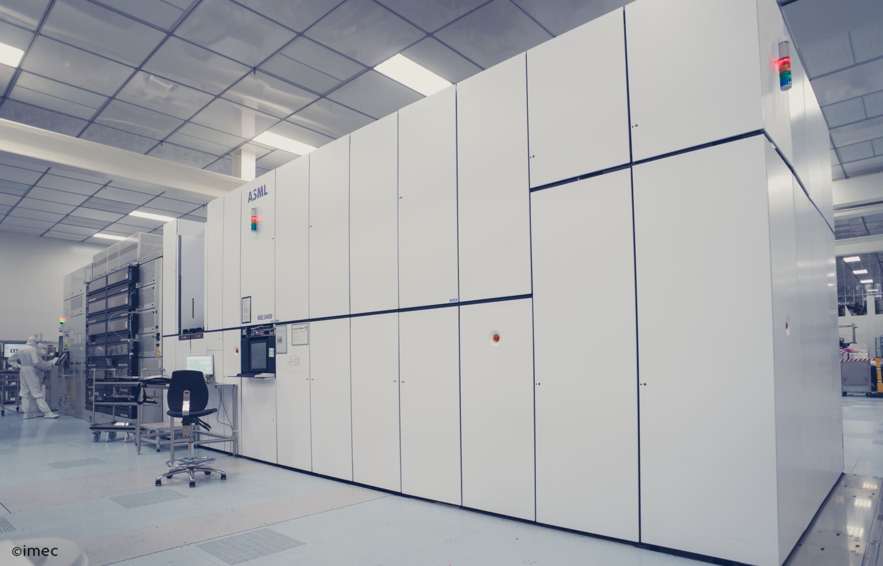
High-NA EUV lithography is a great opportunity for imec – in partnership with ASML – to help our partners accelerate the introduction of the next generation of patterning technologies.
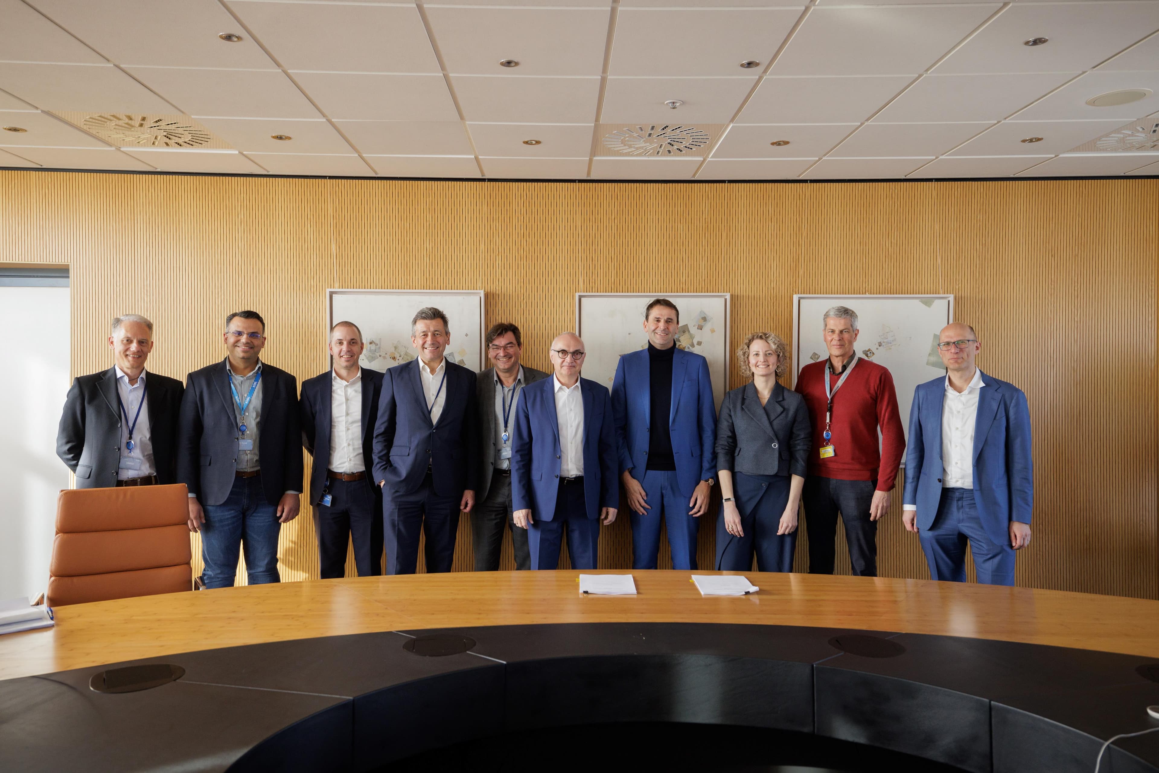
In that context, we are partnering with ASML to open the high-NA lab and create the ecosystem for the industry to jointly address the process challenges that go along with tool development – including anamorphic imaging, new mask technology, improved optical proximity correction (OPC) techniques, materials development for thin film patterning, metrology etc. In this unique joint research lab, ASML and imec will perform research on the manufacturing of the most advanced nanoscale devices by high-NA EUV and assist the ecosystem of equipment and material suppliers to prepare for the introduction of high-NA EUV technology to the industry.”
Which other trend will mark your research domain in the coming years, and how will imec respond to this?
“In the coming years, we expect to see a continued evolution in the field of photoresist materials, which for a long time has been centered around chemically amplified resists (CARs). CARs have been intensely used since the early 1990s and have been gradually optimized for better resist performance. In all these years, imec has focused on supporting the material suppliers in the development of these photoresist materials. More recently, we see an emergence of novel photoresist materials such as metal oxide resists. The introduction of such new materials is very disruptive. Imec enabled multiple material suppliers to develop these concepts and assessed critical issues such as contamination risks and process integration challenges.
A new phenomenon we discovered as the first was the appearance of stochastic failures. We have been developing methodologies to systematically quantify the defect levels in the EUV materials and learn about the many factors contributing to the failures. Key was the development and improvements in the wafer inspection strategies, both optical and e-beam based. These methodologies were offered to the material suppliers testing their newest samples at imec.
The advent of high-NA EUV lithography with further increasing resolution and reduced resist thickness requirements will further drive this evolution.
This is one of the reasons why imec decided to invest in Attolab, a joint project with KMLabs, which will allow us to explore the fundamental dynamics of photoresist imaging under high-NA EUV lithography conditions.
With these insights we will be able to help partners understand and optimize the resist materials to further accelerate the development of the high-NA patterning ecosystem.”
Which application domains do the innovations in EUV lithography relate to?
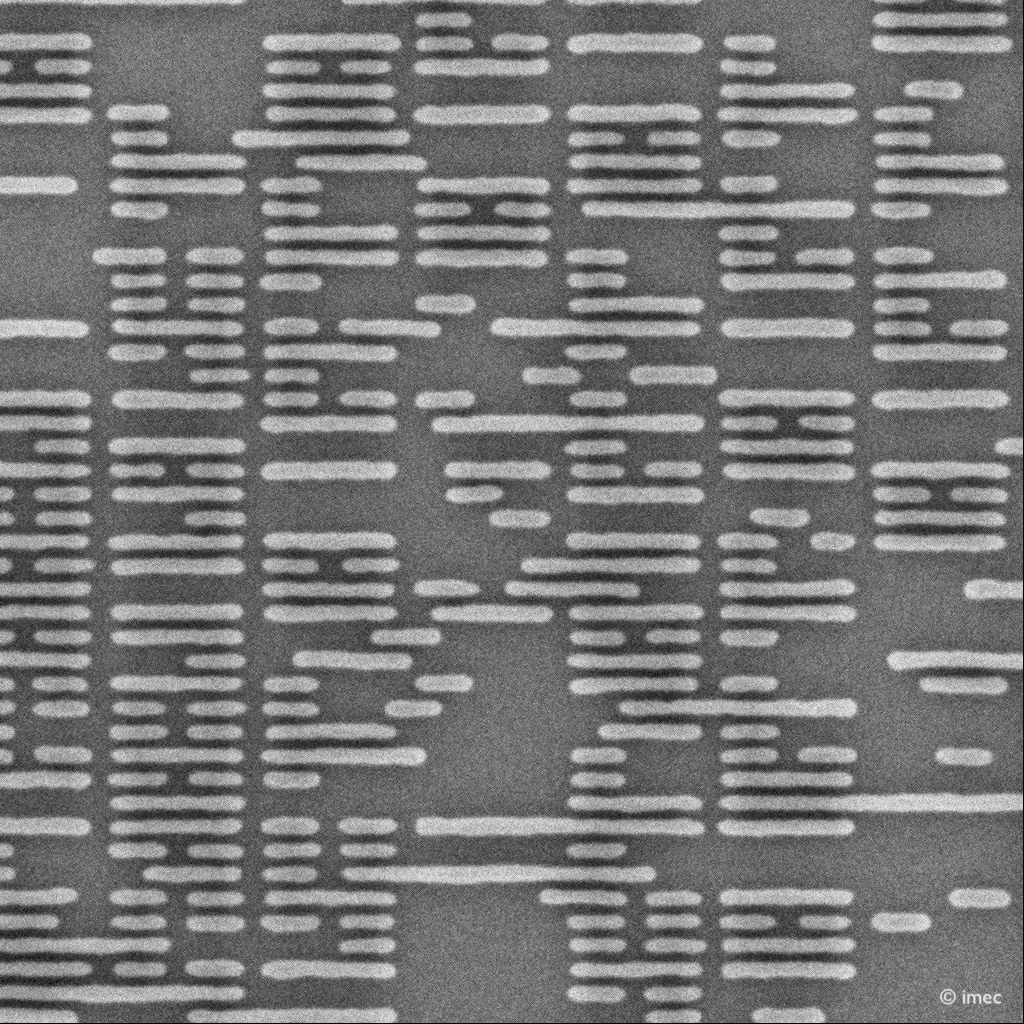
“The insertion of EUV lithography was initially focused on applications in logic technology. For example, in 2019, EUV lithography moved into high-volume manufacturing for printing the most critical metal layers and vias of the 7nm logic back-end-of-line, with metal pitches in the range of 36-40nm. Single as well as multi-patterning options are being explored to advance to the next logic nodes. But in recent years, we have seen an increasing interest from our memory partners in using EUV lithography for meeting the high-density requirements for future memories – for example for patterning critical DRAM structures. For that reason, we recently introduced DRAM patterning in our patterning program and started to develop an ecosystem around EUV in the context of memory.”
Which breakthrough did your team recently achieve, and what is the relevance for industry?
“Together with our partners, we recently achieved several breakthroughs in pushing the capabilities of current and future patterning technologies to their extreme limits – breakthroughs that will be announced at the 2021 SPIE Advanced Lithography conference. One important achievement that I would like to highlight relates to our carbon nanotube (CNT) pellicle. The development of a pellicle suitable for EUV lithography is not straightforward. A major challenge is to make the pellicle absorb as little as possible in order to maintain the throughput and economics of the EUV lithography scanner. In addition, the pellicle must be able to survive exposure to the EUV power of future generation EUV lithography tools. Because there is no high-transmission pellicle solution, some chipmakers forego the use of a pellicle and suffer the resultant yield and process control implications. Imec, in collaboration with our partners, has developed an innovative CNT-based pellicle that has potential to survive scanner powers beyond 600 Watts. The CNT pellicle feasibility was successfully demonstrated through use on an EUV scanner at imec. We are now working to extend the lifetime to enable a high-productivity pellicle solution for next-generation EUV lithography tools.”
Which other avenue(s) is imec exploring to remove primary roadblocks for scaling?
“I would like to answer this question in the context of materials development in general, another area of focus for my team. For many years, materials development has been at the basis of new devices and technologies. Although material engineers have explored almost every single element of the periodic table, new materials and composites will continue to drive the logic and memory scaling roadmaps – albeit with greater complexity. We have started to explore the tremendous possibilities in terms of functional switches of a few monolayers of two-dimensional materials. These materials and their associated interfaces offer a fantastic toolbox to enable further device scaling. In the past, the down-selection of novel materials and interfaces were mainly driven based on simulation insights.
We recently decided to complement our material screening capability by investing in a unique materials and interface lab infrastructure.
This lab will enable the rapid and efficient experimental testing of the materials that look most favourable from simulations. From that lab environment, we will be able to transition them into the 300mm fab and bring value to our partners.”
What makes imec unique for the global semiconductor industry?
“The first time I came to imec was not as a new employee but as a partner, as part of the former company I worked for. It was my first partner technical week (PTW), and I walked away saying: this is different. What immediately struck me about imec is the focus on partnership, in the true sense: the focus on creating an impact for imec’s partners. This partnership model was and still is unique to imec, where everyone could work towards their own goals, both benefiting from, while simultaneously contributing to the ecosystem. It’s a community that allows partners to work together towards solving the industry’s biggest challenges. I think that’s the true spirit of imec, one that attracted me to work with imec, and one that finally also brought me to work at imec.”
Want to know more?
Read our recent press releases on patterning:
Published on:
23 February 2021
