This is the first part of a two-part series dedicated to chiplets. The series addresses recent developments in interconnect technologies (part I) and testing strategies and standardization efforts (part II).
This article first appeared in 3DInCites. You can find it here.
Chiplets, beyond the hype
Ranked by MIT Tech Review as one of ten breakthrough technologies of 2024, chiplets have made quite the entrance into the semiconductor world.
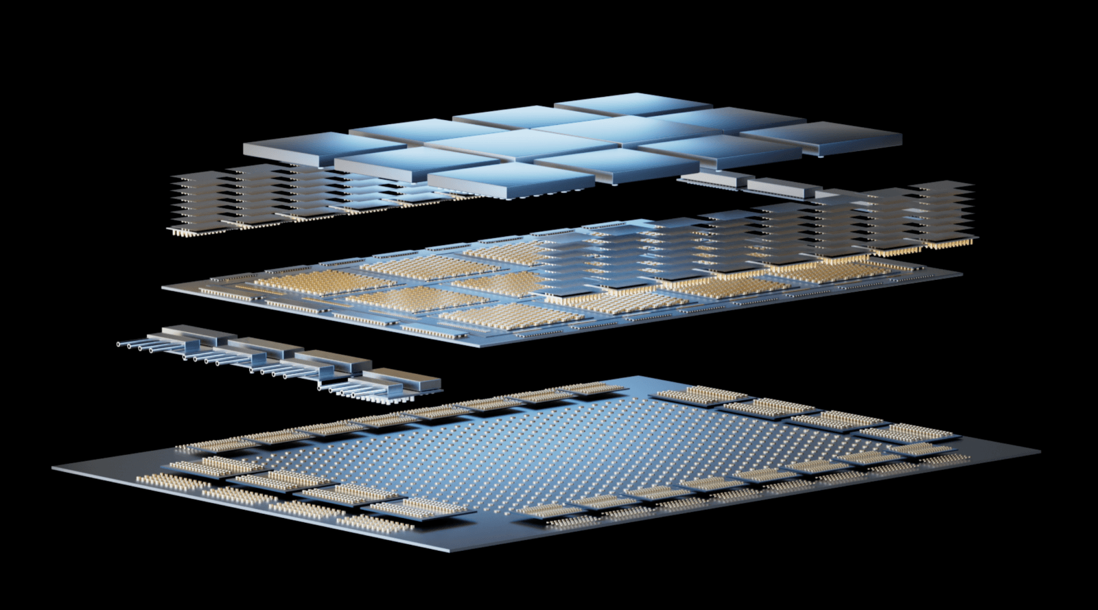
Chiplets are small, modular chips serving a specific function, such as CPUs or GPUs that can be mixed and matched into a complete system. The Lego-like approach hands manufacturers the flexibility to compose a system cost-effectively with lower entry costs for new chip designs and increased efficiency and performance.
One way chiplets achieve optimization is by tailoring technology strategically. For example, IO and bus chiplets use reliable legacy nodes, while compute chiplets employ cutting-edge technology for peak performance. Memory chiplets embrace emerging memory technologies, ensuring adaptability to diverse semiconductor demands.
Additionally, chiplet-based designs accelerate the development process because outdated chiplets can easily and more frequently be updated. Finally, chiplets typically boast high yield rates because they are often smaller with simpler designs, they start with known good dies after pre-bond testing and they can rely on repair strategies for defective interconnects.
Fragmenting large monolithic system-on-chips
Chiplet-based designs answer the slowing down of Moore’s Law that has fueled the semiconductor industry for the past decades. To ensure the biannual doubling of components on integrated circuits, chipmakers explored ways to make transistors smaller and cram more onto chips, resulting in sizeable monolithic system-on-chip (SoC) designs. Mobile phones are a testament to the success of monolithic designs, combining mathematical functions, display, wireless communication, audio, etc., all into one single 100mm2 chip.
However, further scaling grew tremendously expensive for a minimal performance advantage. Hence, the idea is to divide the large, complex SoC into smaller chiplets and link them together to build a system for specific applications.
The automotive industry is a perfect candidate for adopting chiplets offering a flexible electronic architecture with a base function chiplet augmented with specific components, including chiplets for autonomous driving, sensor fusion, and other electronic functions.The modular approach shortens the time to market, replacing or updating chiplets in the lifetime of a vehicle line compared to the lengthy process involved in upgrading a monolithic SoC.
Moreover, automotive sales, especially when looking at specific car models and types, have smaller volumes than, for example, mobile phone. Consequentially, redesigning (parts of) a monolithic SoC for each of these car models would result in high engineering costs.
Finally, the flexibility chiplets offer also helps car manufacturers meet reliability and safety requirements with dies that have already been proven in other car designs.
Explore imec's automotive chiplet program
With the chiplet market ramping up, these modular designs are expected to appear in many more application fields, such as imagers, displays, memory, and quantum computing.
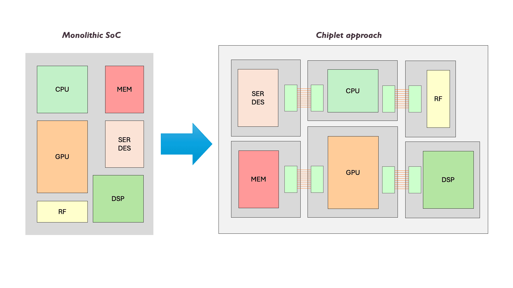
Figure 1 - Chiplets offer a modular system that combines separate chips from different vendors and technology nodes instead of designing all functions into one monolithic system on chip.
Do you want regular updates on imec’s semiconductor research?
Chiplets: (inter)connecting the bricks
Whether or not chiplets will succeed in keeping pace with Moore’s Law largely depends on how close chiplets can be placed together in one package to ensure fast, high-bandwidth electrical connections between them just like the functions in monolithic SoCs.
Two major industry directions are emerging in 3D system integration: 2.5D chiplet integration connecting chips side-by-side through a common substrate (also known as an interposer) and 3D-SoC, where the chiplets are stacked on top of each other.
2.5D interposer technology
In 2.5D integration, the chiplets are connected via a common substrate in silicon, organic polymers, glass, or laminated.
Imec is currently focusing on silicon and organic substrates. While silicon interposers are an established technology for high-performance applications featuring the finest pitch and good thermal and electrical properties, they also come with higher cost and complexity. Organic substrates are therefore researched and optimized as alternatives.
Early chiplet integration was focused on using silicon interposer substrates for interconnect between dies. It involves placing two separate chiplets very closely together (<50µm apart) on the common interposer, a substrate with micrometer-scale wiring that establishes the connections. Silicon interposers utilize traditional BEOL Cu/oxide damascene to realize µm and sub-µm level interconnect pitches with very high yield.
While this remains a valid approach, alternative techniques are gaining interest as they may result in more cost-effective solutions. One option imec offers is a silicon “bridge”, a small silicon interposer that only connects the chiplets together at the edges.
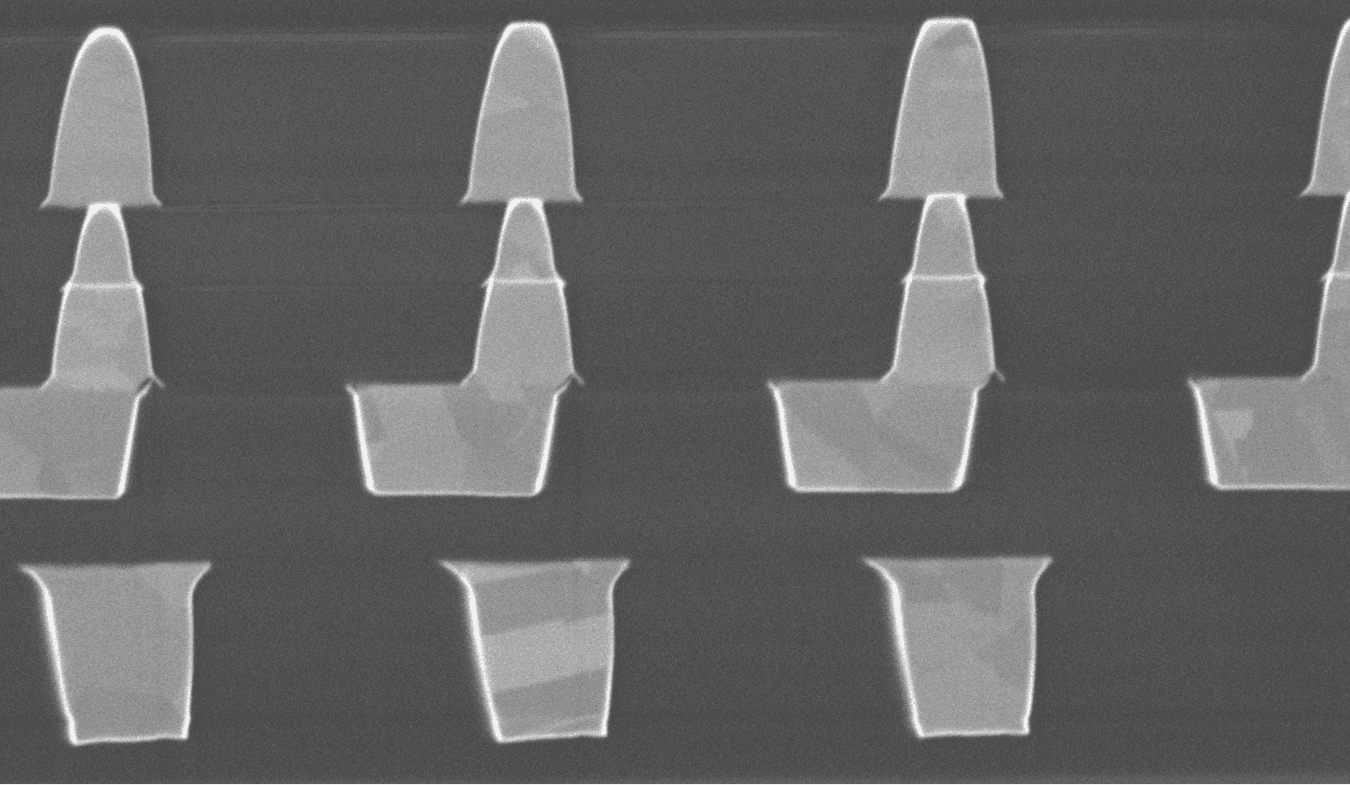
Another alternative, the ultra-fine Redistribution Layer (RDL) interconnect technology, replaces silicon with organic polymers, which embed a layer of copper lines for connecting the chiplets. Imec is currently optimizing this technology, working on reaching a similar interconnect density as with its silicon counterparts and improving compatibility with silicon. Regarding pitch, interposers still hold first place with submicron pitches; imec is targeting 2µm pitches for RDL and even submicron further down the road.
Figure 2 - Chiplets can be integrated using a silicon interposer. Imec is also researching alternatives like silicon bridges or organic RDL.
Next to exploring alternatives to silicon interposer technology, imec is also researching ways to make the interposer a more valuable component by adding extra functionalities. For example, an interposer can have an additional decoupling capacitator to protect chiplets from noise and power anomalies.
3D system-on-chip: hybrid bonding realizes submicron pitches
Some applications, such as high-performance computing, may demand high performance, smaller form factors, or a higher level of system integration and, therefore, prefer a complete 3D approach. Instead of establishing sideway connections, chiplets can be stacked on top of each other, forming a 3D-SoC. This approach does not add additional blocks but rather co-designs the chiplets together and lets them operate as if they would be the same chip.
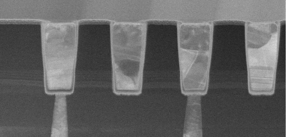
Wafer-to-wafer hybrid bonding is a key technology for integrating 3D-SoC at the µm interconnect density level. It involves connecting two silicon chip(let)s with a low-temperature expansion coefficient together. The critical component in this process is the dielectric that planarizes and activates the surface of stacked layers for effective bonding and electrically insulates the different chiplets in the stack. Imec’s proprietary approach deploys SiCN as a bonding dielectric, scaling down interconnect pitches to 700nm. The roadmap even forecasts pitches of 400nm and 200nm.
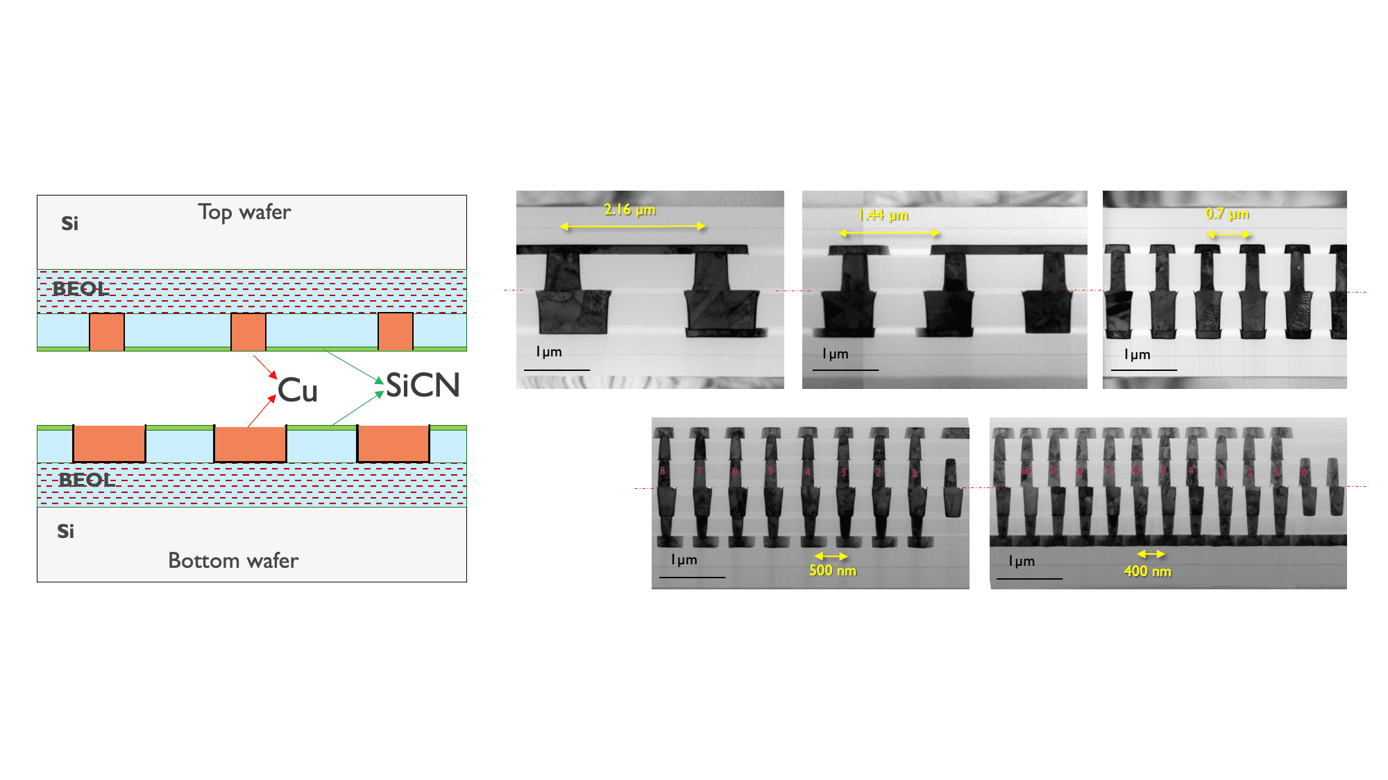
Figure 3 - Wafer-to-wafer hybrid bonding is a key technology for integrating 3D-SoC at the µm interconnect density level. Imec’s proprietary approach using SiCN as a bonding dielectric manages interconnect pitches scaling down to 400nm pitch.
Microbumps versus hybrid bonding
For 2.5D technology, chiplets are placed on top of the interposers using small solder bumps that create the electrical and mechanical connections. The finer the pitch between those microbumps, the faster and more stable the connection. Microbumps in industry typically reach a pitch between 50µm and 30µm. Imec is researching how to decrease the pitch to 10µm and even 5µm.
Compared to the microbumps used in 2.5D, hybrid bonding in a 3D stack yields substantially smaller pitches. Is it possible to use hybrid bonding everywhere, then? Indeed, in a die-to-wafer approach (silicon-based), chiplets can be bonded to a silicon interposer, reaching pitches of a few µm. Not 200nm, as the best die-to-wafer placement accuracy currently approaches 250 nm, while the leading-edge wafer-to-wafer bonding can go down to 100nm overlay accuracy. Improvements in bonding equipment and related processes are expected to further decrease these numbers by 50 percent. Still, hybrid bonding involves additional processing steps, such as surface activation and alignment, which can impact manufacturing costs.
Wafer-to-wafer bonding, die-to-wafer bonding, and microbumps will coexist in a trade-off between cost, pitch, compatibility, and interoperability. In 2.5D, chiplets often come from different vendors and have already undergone a series of tests and manipulations. Microbumps will be the preferred choice as they offer a standardized method that does not require surface preparation. Also, for organic RDL, microbumps are still preferred as organic polymers expand more with heating and cannot be planarized sufficiently.
Concluding thoughts
As scaled technology gains complexity and drives up design and processing costs, it becomes more challenging for smaller-scale applications – think of the plethora of models and types in the automotive industry – to develop dedicated SoCs in the most advanced technology nodes. Separating functions and technology nodes into different chiplets proves more cost-effective and has space and performance benefits over huge chips in cutting-edge process technologies.
While a modular approach provides answers to the complexity and cost of multichip packaging, this paradigm shift brings about specific technological challenges. Size is just one challenge. A substantial part of chiplet research is dedicated to making the interconnections smaller and/or exploring different concepts of bringing the pieces together. When stacking chiplets together, thermal issues and power delivery (tackled by novel architectures such as backside power delivery networks) become critical. Finally, further standardization efforts are needed to ensure compatibility and communication between different chiplets.
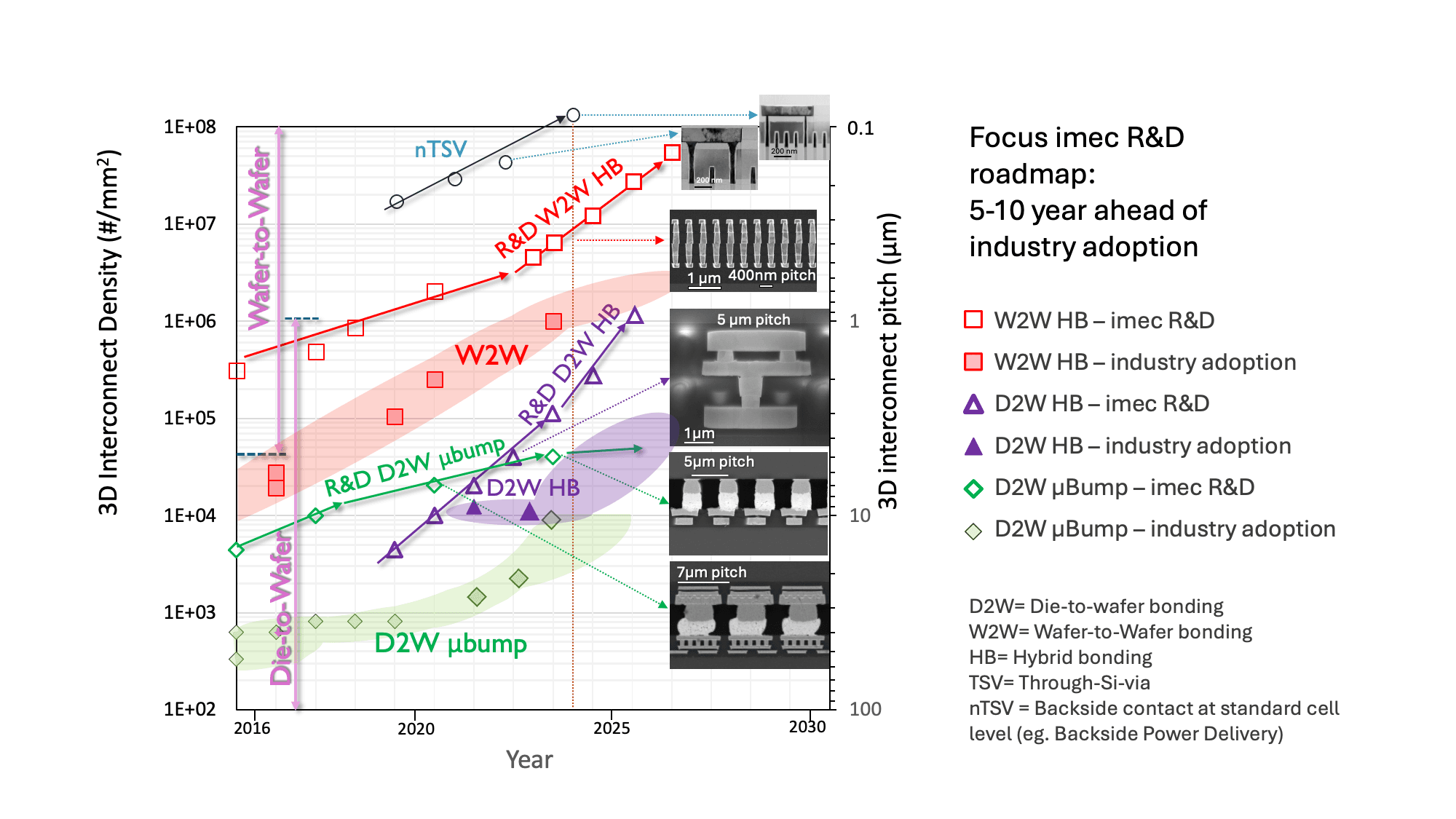
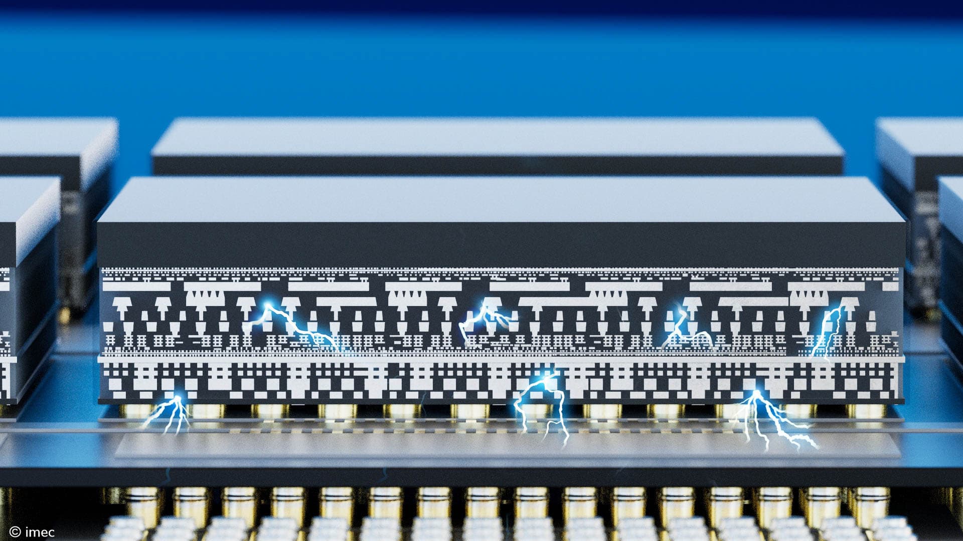
Figure 4 - The 3D interconnect roadmap from imec summarizes the different approaches to interconnect chiplets and projected interconnect densities and pitches.
Want to know more?
- Read more about how chiplets can transform the automotive industry. You can also find information on imec’s Automotive Chiplet Alliance on the dedicated page.
- This article focuses on imec’s wafer-wafer hybrid bonding research.
- Dive into the future of 3D stacks with power delivery from the chip’s backside (backside power delivery network, BSPDN).

Eric Beyne is a senior fellow, VP of R&D, and program director of 3D system integration at imec in Leuven, Belgium. He obtained a degree in electrical engineering in 1983 and a Ph.D. in Applied Sciences in 1990, both from the KU Leuven, Belgium. He has been with imec since 1986, working on advanced packaging and interconnect technologies.

Geert Van der Plas obtained a Ph.D. degree in Applied Sciences from the Katholieke Universiteit Leuven, Belgium, in 2001. He joined imec, Belgium, in 2003. He has been working on energy efficient data converter, power/signal integrity and 3D integration technologies. Currently he is program director of the XTCO Power program addressing system scaling challenges related to power delivery for high performance, energy efficient systems. In the Cross-technology co-optimization (XTCO) program, STCO/DTCO methodology is applied to align technology roadmaps with application needs. Geert’s interests are in system exploration and optimization, modeling and design enablement.
Published on:
16 July 2024


