The healthcare arena is on a clear path towards preventative and personalized medicine. Measurements of health status are essential in advising patients and healthcare professionals on the most appropriate preventive or curative measures. However, our ability to measure our health status is hampered by the complexity, cost and size of instrumentation required to acquire that data, and by the complexity of the analysis required to turn that data into actionable information.
But, semiconductor technologies have excelled at making extremely complex instrumentation and data analytics available at a much lower cost. Semiconductor technology can be tuned to enable health measurements anywhere, anytime, by anyone, and at very low cost.
Silicon to the rescue
The key theme to many advances in today’s healthcare research is highly individualized diagnosis and treatment. Not only will we need new tests that are more precise than anything we have today. We’ll also need to make testing so fast and cheap that we can test and treat all patients whenever there is a need. And this without overstretching the already heavily challenged healthcare budgets. More precise and affordable tests should make treatments more effective and thus will have a positive impact on the healthcare budget.
Here is a chance and a challenge for silicon process technology.
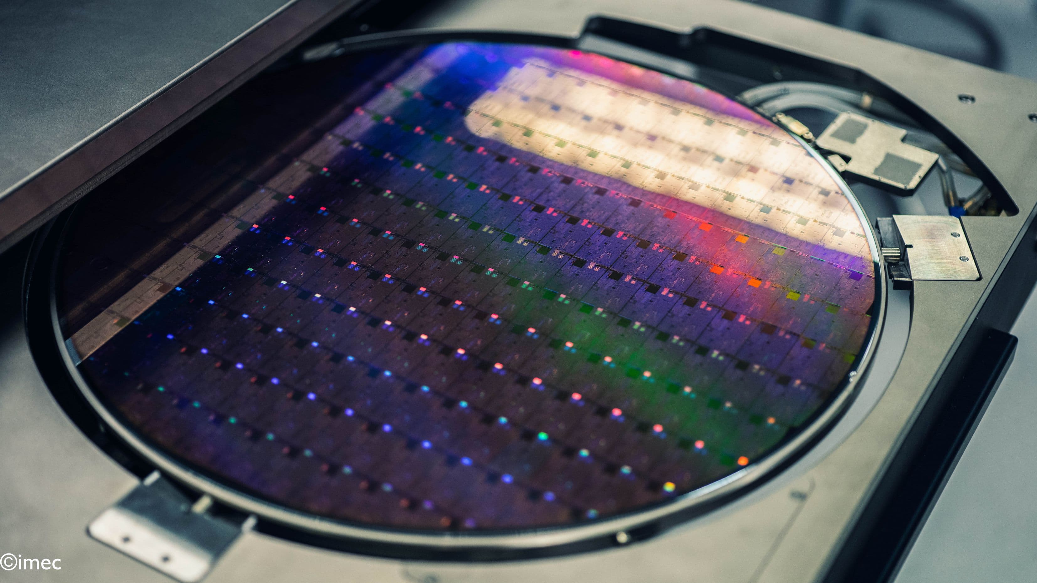
The past decades, we have mass-produced complex electronic chips at ever greater performance for ever lower cost. And while we were doing that, we have also learned how to make silicon work with light, how to make silicon surfaces biocompatible, or how to do micromachining and microfluidics. All using the same cost-efficient manufacturing processes.
Today, we can scale silicon components to the same scale as cells and biomolecules. So we’re reaching out, building an interface between silicon chips and biology. The results we obtain in the labs are picked up by companies and are already integrated in the first commercial products. DNA sequencing machines, miniaturized diagnostic tests using disposable photonic chips, accurate body monitoring sensors, brain stimulation probes ...
Silicon technology is one of the most promising solutions for low-cost, sensitive and specific measurements of a large number of biomarkers. It will play a key role in enabling very powerful instrumentation that will facilitate both discovery in the lab and routine diagnostics anywhere and anytime.

Chip technology has given us ever-faster and smarter computers, smartphones, sensors and will keep on doing this in the future. We will need further scaling of the chips building blocks for faster and better data communication, computation and storage in large server plants. And, last but not least, chip technology will enable a revolution in healthcare.
An extra flavor: silicon photonics
You probably make daily use of photonics: glass fibers make that you can use the internet and watch tv without any problems. These fibers send data with the help of light, which is much more faster and energy efficient than within the standard digital cables.
And, you can do the same on a chip. With ultra-small ‘fibers’ and waveguiding structures you can send light on the chip and make it perform all sorts of tasks such as transporting and manipulating data. Also bio applications are possible. Indeed, light is the most used probe in medical diagnostic testing. Just think of micro- and spectroscopes. Based on light, you can count and visualize cells, measure the characteristics of biological tissues, determine DNA sequences etc. In contrast to datacommunication applications that use near-infrared wavelengths, biological applications use visible light.
Biophotonics on chip is a relatively new research domain that will be very important for diagnostics, therapy and follow up. Doctors will be able to analyze a tissue sample without having to use big (fluorescence) microscope and will study a tissue sample without big spectroscopes.
It is an enormous challenge to make compact optical systems that can perform a medical task in an efficient and reliable way. If you can make your optical circuits out of silicon, just as electronic computer chips, then it becomes possible to integrate the photonic circuits with electronic ones, resulting in a smart and compact system. In fact, in the visible range photonic waveguide materials such as silicon nitride combine easily with standard photodetectors, imagers and sensor arrays. Also, this combination can be mass produced very cost effectively and hundreds and thousands of these sensor systems can work in parallel, resulting in an extremely high throughput of testing.
Based on photonic-electronic hybrid chips, one can make revolutionary healthcare solutions, with the main characteristic of being compact, smart, low-cost and easy to use. Let me give you a few examples of the work we are doing in our research center, imec, that combines the power of integrated photonics and electronics in life sciences.
Electroceuticals and brain probes
One of the examples that explain how healthcare can benefit from silicon technology is in the field of implantable electronics that measure and interact with nerves and brain cells.
Such implants can be used therapeutically. There is, e.g. already a proven technique called ‘deep brain stimulation’ to mitigate tremors in Parkinson’s patients. Other technologies referred to as electroceuticals aim to interact with the peripheral nerve system running through our body, connecting organs. The ultimate goal here is to have a technology that can be used to improve the quality of life of people with neurodegenerative diseases, spinal cord injuries, pain management. These implantable probes need to be thin, flexible and biocompatible threads with thousands of electrodes to transmit and modulate neural signals.
Equally important, we need probes that help us better understand the effect of those electroceutical therapies, probes that can directly measure what goes on in a brain. How healthy neural cells relay signals and react on external stimuli. And how this mechanism is distorted by neurodegenerative diseases such as Alzheimer’s disease. Making such breakthrough probes, we can measure the activity of brain cells of living animals. The silicon-based probes have more integrated electrodes and signal processing than was possible until now. The probes allow to chart brain activity with an unprecedented detail.
Next to these multi-electrode probes, researchers from imec have added another instrument to the brain research toolbox: a probe that can stimulate the activity of brain cells by shining light on them. The probes can be used for ‘optogenetics’, a technique combining genetics and optics. Optogenetics was called one of the breakthroughs of the decade by the magazine ‘Science’ in 2010 and more recently a top 10 emerging technology by the World Economic Forum. With the technique, scientists single out a specific type of cell by adding a string of DNA to its genetic material that makes the cells sensitive to light. This DNA, coming from fluorescent algae, instructs the cells to synthesize a protein that forms an ion channel in the membrane of the brain cells. And that ion channel is light sensitive: light with a specific wavelength will cause the channel to open or close, changing the electrical activity of that brain cell while leaving others unaltered.
Imec finetuned its ‘lightning’ neuroprobes for use with two types of proteins: channelrhodopsin and halorhodopsin. The first reacts to blue light (470nm) and increases the electrical activity of the cell; the second reacts to yellow light (590nm) and decreases the activity of a cell. This technique can be used either in vitro or in vivo to stimulate brain cells very precisely and locally and to measure the effects of stimulation. It’s a unique tool for brain researchers to understand the complexity of the brain.

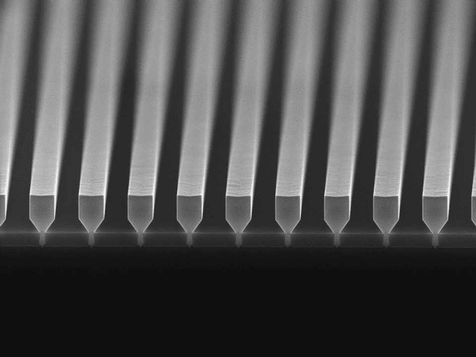
With silicon technology, one can make neuroprobes for therapeutics and brain research, with more integrated electrodes, photonic waveguides and signal processing than standard neuroprobes.
DNA sequencing
Within a foreseeable space of time, determining someone’s genetic code will be as normal as doing a CT scan. Every child will be able to have his or her genetic passport from birth. In fact through prenatal testing of fetal DNA in maternal blood, pregnant woman will get analyzed even before deliver. It will become the foundation for a healthy life. Also, we will be ‘sequenced’ several times during your life. DNA sequencing will become so accurate that you’ll be able to use a blood sample to go looking for ‘rare’ DNA coming from a tumor or an infection. DNA sequencing is the digitization of life.
At imec, we’re developing silicon photonic chips that read DNA molecules in a massively parallel way with minimal preparatory steps. With these chips, DNA sequencing can become a routine diagnostic test. Already today, the cost of the sequencing equipment is falling; the quantity of DNA that can be analyzed per hour – the throughput – is also increasing. We are using our expertise in nanophotonics, CMOS sensors, integration and chip production to improve this equipment. And we are working on it with various major players, too. For example, Pacific Biosciences has been able to reduce the cost of its equipment by 50% and their chips are generating 7 times more information as the result of our working together.
In addition to lowering the cost of the equipment and increasing throughput, we are also making progress towards ‘long reads’ – in which long strands of DNA can be read. This compares with earlier techniques in which the DNA was divided into small pieces, multiplied and then complicated bioinformatic algorithms are needed to restore the information. The advantage of ‘long reads’ is that we can put together a person’s entire genetic map much more accurately and quickly than before. It also makes it possible to detect structural variations. These are pieces of code that are repeated in the genome at specific places. Any abnormalities in this pattern may also lead to health problems.
There are various technologies on the market, as well as equipment in all shapes and sizes – from large DNA-sequencers like they use at Pacific Biosciences, down to small handheld devices such as the MinION from Oxford Nanopore Technologies. So different technologies will live side by side, each one for a different specific market. Small, wearable devices may be important if you want to test diseases such as Ebola in remote areas, whereas the large equipment is useful for producing complete genetic maps quickly and accurately. In all those cases photonic chip technology is particularly important for making these systems more compact, faster and less expensive.
Cell inspection and sorting
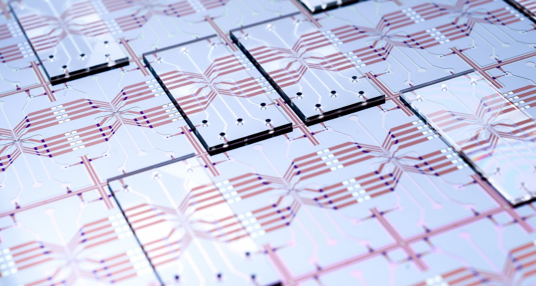
A third example of silicon- and photonics-based innovation for life sciences is the cell sorter chip that imec is developing. It’s a chip-sized detective that may find rare cells in a blood or urine sample in a faster and cheaper way than is possible with existing tools. Moreover, this ‘liquid biopsy’ diagnosis tool will be much more compact than existing tools, and much easier to use and less invasive than interventional biopsies. The secret: a smart combination of silicon photonic technology, lens-free microscopy, and ultra-small steam bubbles.
It would allow medical doctors to do complicated tests on the fly, e.g. screening blood cells in a patient’s blood sample. Think of an oncologist, who would immediately be able to see if a patient has tumor cells roaming in his blood, a potential sign of metastatic cancer. He would regularly check after a patient’s chemotherapy if the number of tumor cells in the blood has diminished, and if the treatment has to be continued or changed. Cured patients will love to screen their blood regularly when the biopsies are less painful and metastasis can be discovered earlier.
Such a high-throughput ‘cell sorter’ chip would not only lead to faster diagnosis. It could also allow a simple way to isolate tumor cells in order to sequence their DNA and start a treatment based on the characteristics of the specific tumor type. Since treating cancer is like chasing a moving target that mutates itself, regular sequencing of these rare cells becomes increasingly important to adapt therapies. Or used in stem cell therapy, where patient cells are used for culturing and deriving novel types of cell based treatments, it could be deployed to check the quality of the cells as well as to filter out cells which may be dangerous for patients.
For visualizing and identifying cells, the cell sorter uses optical waveguides to measure cell signals. A waveguide illuminates the cells in the fluidic channel one by one as they pass. An image sensor placed under the channel captures the emitted or scattered pattern of the light that has passed through the cells.
A microfluidic switch is used to separate the cells of various types. The switch is based on small, star-like heating elements. These heating elements create steam bubbles that push the cells into the right channel. Sorting with these jet flow generators takes about 100 microseconds per cell. Both this speed and the fact that no moving elements are used, is a great advantage of this device for robust and automated cell processing.
This concept and prototype of a cell sorter becomes extremely powerful if you consider the parallelization that is possible with the silicon chip technology. Whereas the first prototype had only one microfluidic channel, the next ones were extended to tens or even hundreds of channels that function in parallel and thus can sort hundred thousand and even millions of cells. That way, it becomes possible to attain an unseen throughput for cell analysis and sorting.

‘Cell sorter’ 5 channel flow cytometry chip that identifies and sorts 5,000 cells per second per channel.

Liesbet Lagae is co-founder and currently Program Director of the Life Science Technologies in imec. In this role, she oversees the emerging R&D, the public funded activities and early business creation. She holds a PhD degree from the KU Leuven, Belgium for her work on Magnetic Random Access Memories obtained under an IWT grant. As a young group leader, she has initiated the field of molecular and cellular biochips leveraging silicon technologies at IMEC, Belgium. The life science program has grown from emerging activities to a mature business line that provides smart silicon chip solutions to the life science industry. Applications include medical diagnostics, point-of-care solutions, DNA sequencing, cytometry, bioreactors, neuroprobes, implants. She holds a prestigious ERC consolidator grant for developing a platform on single cell analysis and sorting and she coordinates the PIX4LIFE pilot line consortium aiming to port photonic IC technology in the visible range to life sciences. She has (co-) authored 125 peer-reviewed papers in international journals and holds 15 patents in the field. She is also part-time professor in nanobiotechnology at KU Leuven/Physics department.
Published on:
5 July 2017

