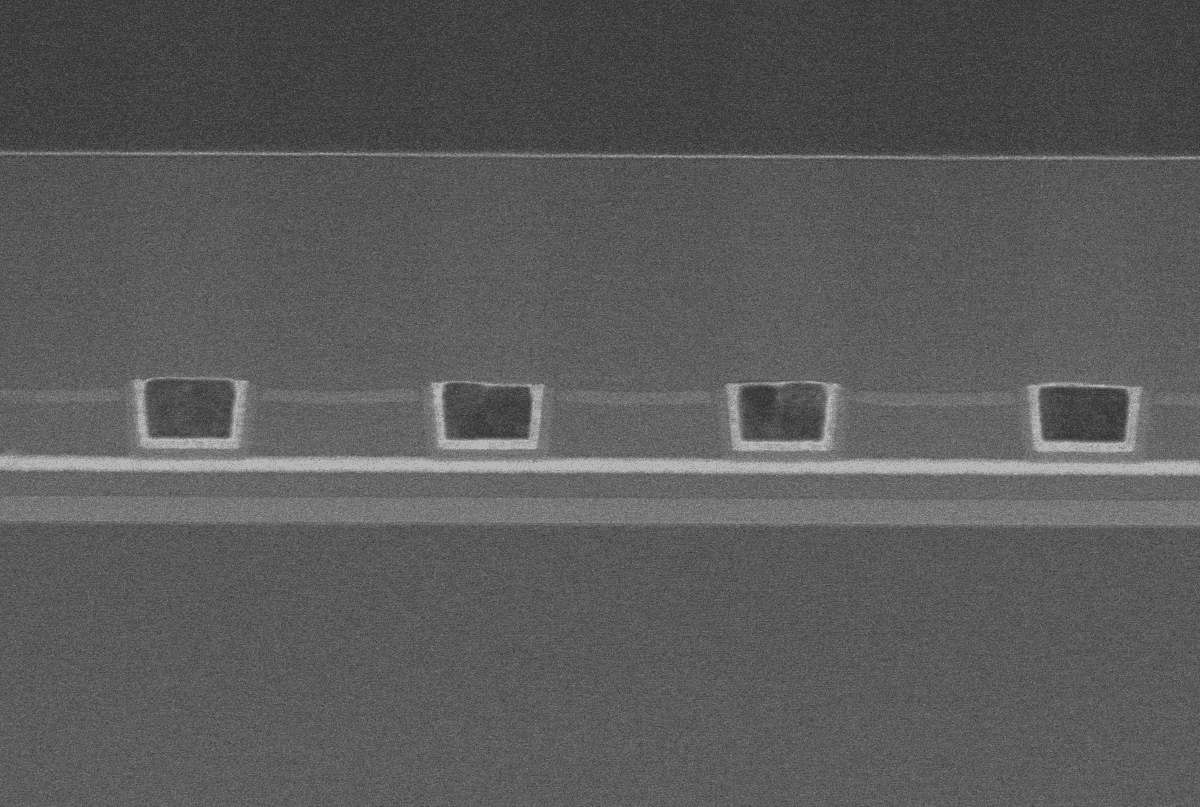
Which are the next challenges in logic scaling that need to be tackled in the coming years?
Sri Samavedam: “In logic CMOS, the node-to-node cost and complexity is increasing at a faster rate than the power-performance-area (PPA) benefit. Both TSMC and Samsung have announced that FinFET logic devices will be replaced by a nanosheet architecture in the coming nodes.
We expect the forksheet device architecture, which is an imec invention, to extend nanosheet generation with additional scaling and performance.
Complementary FETs (CFETs) where the N and P devices are stacked on each other are very promising for SRAM and logic scaling after the nanosheet generations. Beyond CFETs, we are extensively researching 2D atomic channels where many fundamental materials challenges like growth, low resistance contacts and formation of gate dielectrics still need to be addressed. In the back-end-of-line (BEOL), we will need hybrid metallization where the via and line are formed using different metals to address via resistance increase. High aspect ratio metal lines will be needed to lower the resistance increase at smaller pitches. This requires innovations in direct metal etch, moving away from the mainstream copper dual-damascene integration.”
How is imec addressing the mid-term challenges in active memories and storage?
“The scaling of DRAM memories is creating many challenges in cell operating margins which requires innovations in materials, integration and design. New material innovations like ferroelectrics with high polarization could lead to smaller DRAM capacitor areas. We also anticipate an architecture change where the DRAM array will be formed on top of the periphery logic to scale area further. This requires a low off-state leakage transistor like an indium gallium zinc oxide (IGZO) based thin-film transistor. We are evaluating variants of the IGZO family to improve stability and reliability. Together with our partners, we are also researching non-volatile memories (NVMs) based on magnetics like voltage controlled magnetic anisotropy (VCMA) which has the power advantage over traditional spin torque transfer (STT) MRAM. To address the reliability concerns of STT-MRAM, we are evaluating another class of magnetic memories called voltage gated spin orbit torque (VG-SOT) featuring separate read and write paths. On the storage front, we expect 3D NAND to scale by adding more layers to the stack and by reducing the vertical gate length dimension.
To enable 3D NAND scaling we are exploring metals like Mo and Ru for lower word-line resistance, and alternate memory gate stacks.
In addition, we are looking for ways to improve channel mobility and we are addressing potential problems with the next generation 3D trench architecture.”
What about interconnect technologies? How will they influence future systems scaling?
“3D interconnect technologies like wafer-to-wafer Cu-SiCN hybrid bonding or scaled microbumps can enable dense direct connectivity between memory and processing units to improve memory latency and bandwidth in systems-on-chip (SoCs). This will be very power efficient in applications targeting machine learning which requires frequent communication between the memory and compute blocks. Today optical I/Os for datacom applications are based on pluggable optics on the faceplates of the server racks. There is a drive to integrate the optical modules closer to the electrical switches and as such create a system-in-a-package (SiP) with improved speed, cost and energy per transmitted bit. So, innovations in co-integrated optics at the package level or even wafer level are being worked on.”
Does imec also research the sustainability impact of new semiconductor technologies?
“Semiconductor manufacturing uses large amounts of ultra-pure water, chemicals that produce greenhouse gases and tools like EUV machines that consume a substantial quantity of electricity. Increase in complexity of technology nodes complicates the task of estimating the environmental cost of technology choices.
We have developed a framework to evaluate the environmental impact of process flows in the pathfinding phase.
In this phase we typically evaluate the PPA value proposition of a new logic node definition. We have taken the imec process cost models to include sustainability metrics like power consumption, ultra-pure water consumption and greenhouse gas (GHG) emissions. This framework creates awareness about the environmental impact and allows fabs to make sustainable choices early in the technology definition phase. While today’s work focuses on logic process flows, we plan to expand this framework to include NAND and DRAM flows in the future. We also plan to identify process options that are more environmentally friendly.”
What makes imec unique for the global semiconductor industry?
“Imec is an extra-ordinary place to collaborate and innovate on the most challenging research topics. It has some of the best talent from all over the world. We have new researchers, PhD students and post-docs joining every year who bring new ideas and perspectives.
Imec’s research is shaped by access to the entire eco-system of materials and equipment suppliers, IDMs, foundries, fabless, IP suppliers and system companies.
It is a very dynamic and fertile environment to realize practical solutions to tough research problems. I love the ability to engage with smart people and make connections across the entire partner eco-system. Solutions to system-level problems will come from innovations across multiple domains. I feel extremely fortunate to be exposed to research and progress in fundamental understanding in multiple domains like logic, memory, 3D integration, photonics and new materials.”

Sri Samavedam is Senior Vice President of semiconductor technologies at imec since August 2019, oversees programs in logic, memory, photonics, and 3D integration. Previously, he was senior director at GlobalFoundries, leading 14nm FinFET technology into production and developing 7nm CMOS. Starting his career at Motorola, he worked on strained silicon and other advanced materials. He holds a Ph.D. in Materials Science and Engineering from MIT and a master's from Purdue University.
Published on:
19 April 2021


