A changing memory landscape
Memory is one of the key components in electronic systems where it serves multiple needs – from data storage to caching, buffering, and, more recently, (in-memory) computing. For many decades, the memory landscape has been unchanged, with a clear hierarchy from caching to storage. Close to the central processing unit (CPU), fast, volatile embedded static random access memories (SRAMs) are the dominant memories. Also on chip are the higher cache memories mostly made in SRAM or embedded dynamic random access memory (DRAM) technologies. Off-chip, further away from the CPU, you will mainly find DRAM chips for the working memory, non-volatile NAND Flash memory chips for storage, and tapes for long-term archival applications. In general, memories located further away from the CPU are cheaper, slower, denser, and less volatile.
Despite large improvements in memory density, all these memories are struggling to keep pace with the ever-increasing performance of logic chips and with the tremendous data growth rate. This has driven the exploration of alternative memory technologies, for standalone as well as for embedded applications. Emerging options range from new technologies for cache level applications, new ways for improving DRAM devices, emerging storage class memories to fill the gap between DRAM and NAND technologies, solutions for improving 3D-NAND storage devices and for archival type of applications. One of these emerging memories are magneto-resistive random access memories (MRAMs).
The early days of MRAM research: from lab to space...
While traditional memories such as DRAM and NAND Flash make use of electrical charges to store binary data (0 or 1), MRAM utilizes the collective magnetization state of a ferromagnetic layer. Its core element is a magnetic tunnel junction (MTJ) in which a thin dielectric layer is sandwiched between a magnetic fixed layer and a magnetic free layer. Writing of the memory cell is performed by switching the magnetization of the free ferromagnetic layer – the ‘storage’ layer of the MRAM bit cell. For reading, the magnetoresistance of the MTJ is measured by passing a current through the junction. This tunnel magnetoresistance (TMR) can be high or low, depending on the relative orientation of the magnetizations of the free and fixed layers (i.e., parallel or anti-parallel, and thus 1 or 0).
Figure 1: Principle of the MRAM TMR read operation.
Do you want regular updates on imec’s semiconductor research?
MRAM is surely not a new technology: its development goes back several decades. The first implementations (such as toggle-mode MRAM) relied on magnetic-field-driven switching, where an external magnetic field was applied to switch and write the memory bit cell. This field was generated by passing an electrical current through a Cu wire. It was a fine piece of engineering, but the magnetic-field-induced switching was not scalable towards smaller sizes – as the current required to achieve the desired field increases with the reduction in the size of the current lines. The technology would never enable high-density MRAM applications and was therefore limited to a few niche applications, such as space – for which it is still being used. In space applications, the great advantage of the magnetic-field driven technology can be fully exploited: it is extremely stable and reliable, and it can operate in radiation harsh environments.
Over the years, new ways of writing the technology have been proposed – including thermally assisted switching – but so far without any great commercial success.
... and to the (niche) market
A major step towards the commercialization of MRAMs came about 20 years ago, with the invention of the spin-transfer torque MRAM (STT-MRAM). Other than the classical MRAM, STT-MRAM uses a current to induce switching of the free magnetic layer. By passing a current through the fixed magnetic layer, one can produce a spin-polarized current – which has more electrons of either spin up or spin down. If this spin-polarized current is directed into the free ferromagnetic layer, the angular momentum can be transferred to this layer (the ‘spin transfer torque’), hence changing its magnetic orientation.
A second breakthrough came from the material side, when ferromagnetic CoFeB was introduced as the material for the fixed and free magnetic layers, and MgO for the dielectric barrier. Using these materials gave a boost to the device efficiency, mainly in terms of a higher tunnel magnetoresistance. After many years of research, first STT-MRAM-based products came on the market around 2015, first as a non-volatile buffer for DRAM and solid-state drive (SSD), and later as a replacement for embedded Flash. Since then, major foundries and tool suppliers have been investing significant R&D resources into (embedded) STT-MRAM.
STT-MRAM to replace SRAM cache memories?
Cache memory in general is a very small type of memory that resides close to the processor to enable fast access to data. This type of memory is typically organized as a hierarchy of different cache levels. The role of the cache memory is usually filled by high-speed, volatile SRAM. Throughout the years, the SRAM bit cells – typically made up of 6 transistors – have been downscaled to increase the memory density and hence the capacity of the cache. But below the 10nm technology node, SRAM scaling has become very challenging, due to the increased power dissipation when memories are not active (leakage) and to reliability issues.
Throughout the many years of MRAM research, STT-MRAM has been put forward as a promising alternative for cache SRAM – an evolution that would allow STT-MRAM to break out of the niche markets. It is non-volatile in nature, which means that it retains data even when the system is shut down. This effectively solves the problem of SRAM memories ‘leaking’ energy when they are inactive. STT-MRAM memory cells are also much smaller than SRAM cells.
At the 2018 IEEE IEDM Conference, imec demonstrated the feasibility of introducing STT-MRAM as a last-level (L3) cache memory at the 5nm technology node [1]. The analysis, based on design-technology co-optimization and silicon verified models, revealed that STT-MRAM can meet the performance requirements for last-level caches in the high-performance computing domain. Also, the STT-MRAM cell occupied an area of only 43,3% of the SRAM macro, and the STT-MRAM was found to be more energy efficient as compared to SRAM for high-density memory cells.
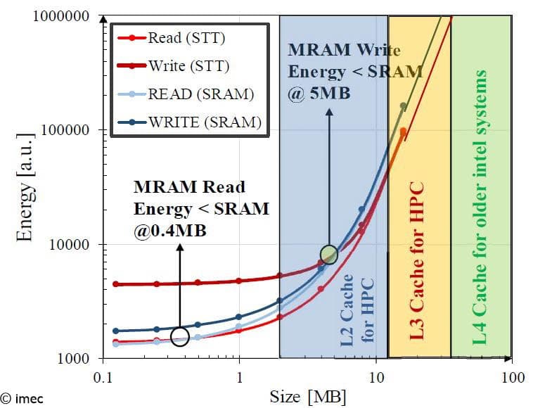
Figure 2: Energy comparison between SRAM and STT-MRAM for varying sizes.
Unfortunately, the technology turned out inadequate to expand operation into the faster, lower-level caches (L1/L2). First, the write process is still relatively inefficient and long compared to SRAM, posing an inherent limitation to the switching speed (not faster than 5ns). Second, speed gains would require an increase of the current flowing through the MTJ, hence through the thin dielectric barrier. This imposes a severe stress and leads to a reduced endurance of the device. These reliability issues in combination with increased energy at fast switching speeds make STT-MRAM memories ineligible for L1/L2 cache operation – which would require sub-ns switching speeds.
The semiconductor industry has therefore been looking for ways to get around these problems, resulting in new MRAM flavors. They all rely on the same mechanism for reading the bit cell (i.e., by measuring the TMR), but differ in the way the memory cell is written. Depending on the writing mechanism, these new flavors (discussed below) perform better in at least one of these metrics: reliability, speed, power and/or area consumption.
Besides exploring innovations on the architectural and material side, it is imec’s major role to make these MRAM flavors manufacturing friendly, by developing CMOS-compatible 300mm-based integration flows. Focus of the team is on MRAM-type of devices with perpendicular magnetization, since it presents much better scaling potential compared to in-plane magnetization technology.
SOT-MRAM: reliable, fast, energy-friendly, but large
From architectural point of view, the main difference between STT- and spin-orbit torque (SOT)-MRAM devices lies in the current injection geometry. In an STT-MRAM device, the current needed to write the memory is injected perpendicularly into the MTJ. For SOT-MRAM, current injection is performed in-plane, in an adjacent SOT layer – typically a heavy metal. In physics terms, switching the free layer now relies on the transfer of the orbital angular momentum from the heavy metal’s electron to the magnetic storage layer – further assisted by the Hall effect and Rashba interaction. The main advantage? Because of the current injection geometry, the read and write path are now de-coupled, significantly improving the device endurance and read stability. It also removes the switching delay that was inherently present in the STT-MRAM device.
While SOT-MRAM device operation has been proven in the lab, imec was the first to demonstrate in 2018 full-scale integration of SOT-MRAM device modules on 300mm wafers using CMOS-compatible processes. This also allowed the team to compare SOT and STT switching behavior, with the devices being fabricated on the same 300mm wafer. While switching speed during STT-MRAM operation was limited to 5ns, reliable switching down to 210ps was demonstrated during SOT-MRAM operation. The SOT-MRAM devices showed excellent endurance (>5x10¹⁰) and operation power as low as 300pJ. In these devices, the magnetic tunnel junction consisted of a SOT/CoFeB/MgO/CoFeB/SAF perpendicularly magnetized stack, using beta-phase tungsten (W) for the SOT layer. [2]
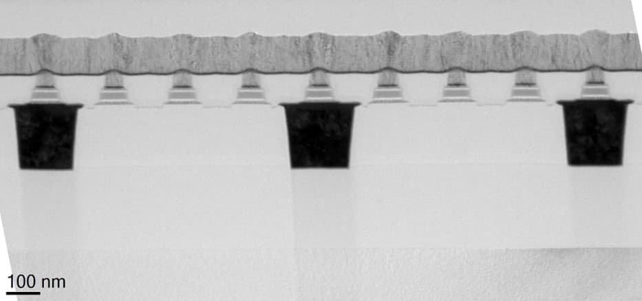
At VLSI 2019, the team proposed a key innovation that allowed to further improve the manufacturability of the SOT-MRAM device: field-free switching operation to eliminate the need for an external magnetic field during write operation [3]. A magnetic field is required to break the symmetry and ensure deterministic magnetization switching. So far, this field was evoked externally, presenting a major hurdle for the practical use of SOT-MRAM devices. Imec’s solution consists in embedding a ferromagnet in the hardmask that is used to shape the SOT layer. With this ferromagnet, a small homogeneous in-plane field is induced on the free layer of the magnetic tunnel junction. The approach was shown to be reliable while preserving the sub-ns writing of the SOT-MRAM device. In addition, it allows optimizing separately the properties of the magnetic tunnel junction and the conditions of the field-free switching.
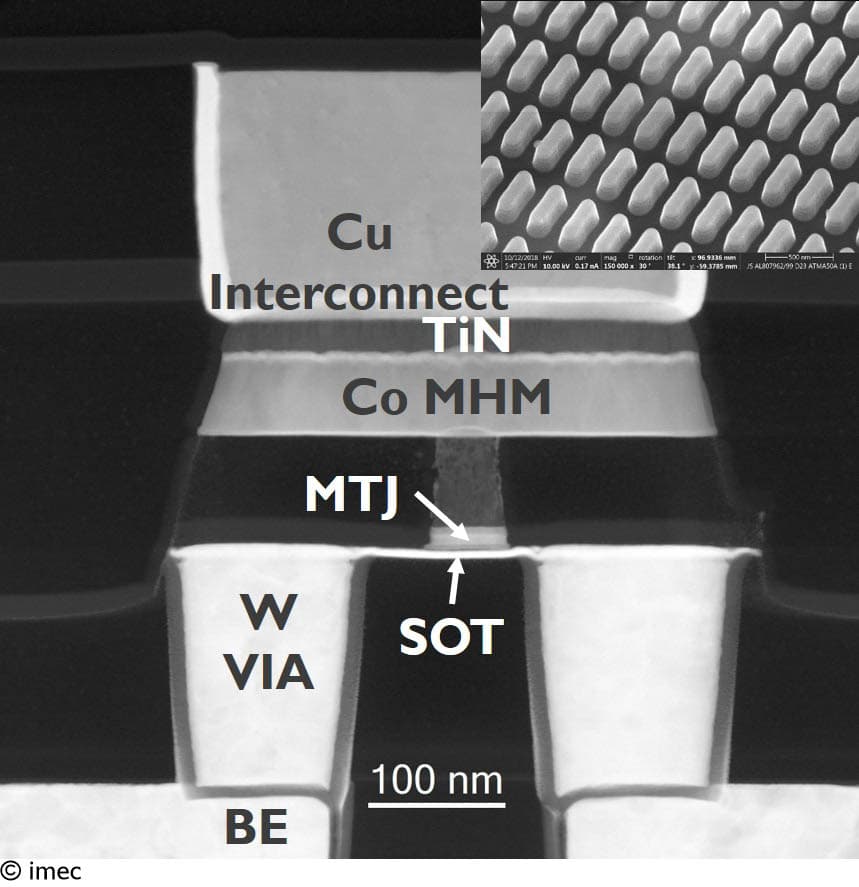
Figure 3: Lateral TEM cross section view of the SOT field-free switching MTJ with Co magnetic hard mask.
Another concern towards manufacturability relates to the thermal budget: the thermal budget for processing the magnetic layers must be compatible with the overall manufacturing flow. At VLSI 2021, imec demonstrated a back-end-of-line (BEOL) compatible SOT device by using a new design for the free layer which provides more flexibility to increase the retention time of the memory [4].
Although these results open the path to address SRAM replacement in the lowest cache level, SOT-MRAM still suffers one main drawback: area consumption. While STT-MRAM with its pillar-like structure is a two-terminal device, SOT-MRAM is a three-terminal device – incorporating two transistors into a unit cell and a relatively large selector transistor (to accommodate the relatively large current needed to write the device). Therefore, innovations in density scaling are needed to make it a true competitor for SRAM in low-level cache applications.
VCMA-MRAM: champion in ultra-low power
Voltage-controlled MRAM operation has been explored as a way to further reduce the power consumption of STT-MRAM. While writing an STT-MRAM memory cell is performed by means of a current, voltage-controlled magnetic anisotropy (VCMA)-MRAM uses an electric field (hence, a voltage) for its write operation – which is far less energy consuming. Two basic components are required to switch the free layer from the parallel (P) to the antiparallel state (AP) (or vice versa): an electric field (across the tunnel barrier) to remove the energy barrier, and an external in-plane magnetic field for the actual VCMA switching.
Although promising in terms of power consumption, this flavour of MRAM typically suffers from a relatively slow write speed. The slow write operation relates to the unipolar nature of the VCMA-MRAM device: the same polarity of write pulse is needed to transition from the parallel to the anti-parallel (P-AP) state as to switch from anti-parallel to parallel (AP-P) state. Therefore, the memory cell needs to be ‘pre-read’ to know its state before writing – a sequence which significantly slows down the write operation.
In 2020, imec introduced a unique deterministic VCMA write concept that avoids the need for pre-reading: distinct threshold voltages are introduced for the A-AP and AP-P transitions by creating an offset in the energy barrier. This offset is realized by implementing a small (e.g. 5mT) offset magnetic field (Bz,eff) in the VCMA stack design. [5]
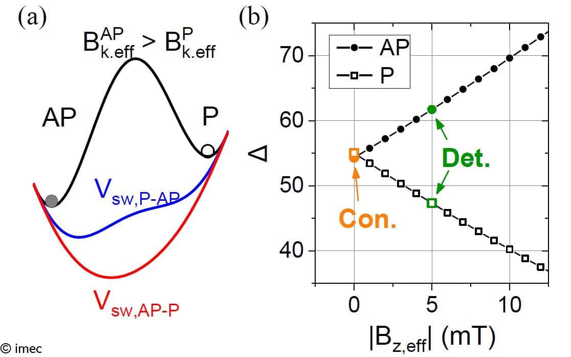
Figure 4: (a) Energy diagram with Bz,eff for the proposed deterministic write, where the AP state is more stable than the P state; (b) retention (Δ) as a function of Bz,eff.
As a second improvement, imec embedded a magnetic hardmask on top of the magnetic tunnel junction. This eliminates the need for an external magnetic field during VCMA switching, improving the device’s manufacturability without degrading its performance. [5]
The resulting devices were fabricated using imec’s 300mm state-of-the-art technology infrastructure, proving their compatibility with CMOS technology. Reliable 1.1GHz (or ns-scale speed) external-magnetic-field-free VCMA switching was demonstrated with only 20fJ write energy. A high tunnel magnetoresistance of 246% and an endurance of more than 1010 have been achieved. These improvements bring VCMA-MRAM performance beyond STT-MRAM operation, making the devices ideal candidates for high-performance, ultralow-power and high-density memory application.
One of the main remaining challenges is related to increasing the magnitude of the VCMA effect. With the current material set, only low-retention (days to weeks) free layers can be switched. Switching high-retention free layers requires a higher VCMA effect, which still calls for material breakthroughs. This field is actively pursued on the established 300mm VCMA-MRAM platform at imec.
VG-SOT promises to have it all
Recently, a new writing scheme was proposed that combines the advantages of both the VCMA and SOT effects: the voltage-gate assisted spin-orbit torque MRAM device (VG-SOT MRAM). In such a device, the SOT effect is again responsible for switching the free layer. But the VCMA top gate now assists its operation, acting as the MTJ selector. The selection is performed by applying a voltage, which subsequently alters the stability of the free layer, thereby changing its retention. With this concept, one can now think of a multi-pillar cell structure (with multiple MTJ pillars on a common SOT line) whereby one single VCMA top gate selects which one to write. This concept promises to address the density limitation of classical SOT technologies, which require a large selector per bit cell. In addition, just like the conventional SOT, VG-SOT enables fast switching in the sub-ns regime. VG-SOT therefore has all the features to play a role in any category of cache – promising to enable a true unified cache memory.
But the road towards industrial adoption is a long one. The device is complex to make, and its full functionality in a multi-pillar structure still needs to be demonstrated. Imec is taking gradual steps towards this goal. The VG-SOT concept on a single 3-terminal device could already be successfully demonstrated on a 300mm wafer, using a perpendicular MTJ building block. Imec is now working towards proving full functionality of a multi-pillar device structure, fabricated with CMOS-compatible process steps.
The VG-SOT device concept reduces the material properties requirement in SOT and VCMA efficiencies vs its standalone counterparts. Still, innovations need to come from the material side to make the device more efficient. New materials with a higher spin-orbit transfer effect are being explored for the SOT layer, aiming at reduced energy consumption. In addition, materials with a larger VCMA coefficient are being looked for. This coefficient determines how much you change the retention when a voltage is applied. In addition, to further improve the TMR readout, fundamental research on alternatives for MgO in the MTJ stack is highly relevant.
Figure 5: Principle of single-pillar and multi-pillar VG-SOT operation.
The potential of (VG-)SOT MRAM for analog in-memory computing
The VCMA-assist multi-pillar SOT-MRAM is also considered an interesting candidate for implementing multi-level deep-neural network weights for analog in-memory computing.
Deep learning is a subset of machine learning where artificial neural networks – algorithms inspired by the human brain – learn from large amounts of data. Neural networks contain a series of hidden layers which apply transformations to the input data. It is within the nodes of these hidden layers that weights are applied, learnable parameters inside the network that transform the input data. Analog in-memory computing is a promising architectural solution to implement the neural network weights. For that purpose, different types of memories are being explored, including low-power, non-volatile resistive memories with large resistance values.
SOT-MRAM promises to fulfill these requirements. Thanks to the separate write and read paths, the resistance of the MTJ stack can be increased without influencing the write path. This way, a very large resistance – and hence, a very low current through the tunnel junction – can be obtained. When using a multi-pillar SOT-MRAM structure, the currents coming from the different MTJ pillars can now be summed up (the actual in-memory computing). This overall current generates the analog signal that serves as the weight for the input signal. As the individual currents coming from the different SOT-MRAM cells are low enough, the final added-up current is still workable.
At VLSI 2021, imec could for the first time demonstrate the feasibility of using multi-pillar SOT-MRAMs (with selective VCMA-assisted writing) to implement multi-level deep neural network weights. Within the experiments, devices with four pillars on one SOT track have been used to implement weights with nine levels. [6]
Outlook: domain-wall devices
On the longer term, imec explores other, more exotic implementations of MRAM devices that promise an even higher density of MRAM bit cells: domain-wall devices. In these devices, input information is encoded in magnetic domain walls, interfaces that separate regions with different magnetization. The device is operated by using the motion of the domain walls along a magnetic track. This motion can be controlled by spin-orbit torque. In such a construct, not every bit cell needs a readout sensor since the domain walls themselves can be routed towards readout units – which are installed at only a few selected locations. As such, a limited number of readouts can be implemented, allowing a significant increase of the density of the memory.
So far, a complete functional domain-wall device could not be experimentally demonstrated due to the lack of electrical means to read and write them at nanoscale. Imec could for the first time demonstrate full operating nanoscale domain-wall devices (fabricated on 300mm wafers), using specifically designed perpendicular MTJs for electrical reading and writing. The results of this study were recently described in Nature Electronics [7].
Besides a high memory density, there is a second advantage of using domain-wall devices for memory applications. Domain-wall devices – in the form of spin torque majority gates – are also considered a further out option for high-performance logic applications. But then you need a platform where logic and memory can come close together. The domain-wall memory can play a big role there, as you can potentially connect logic and memory on the same magnetic tracks.
Conclusion
Throughout the years, different flavors of MRAM memory devices have emerged, trading off writing speed, reliability, power and area consumption. Depending on their specific characteristics, they target different applications, e.g., STT-MRAM for embedded Flash and last-level cache, SOT-MRAM for the lower-level cache memories, VCMA-MRAM for ultralow power applications, and, finally, VG-SOT MRAM as the ultimate unified cache memory, with interesting properties for in-memory computing as well.
In recent years, imec, together with its partners in memory, has proven track record towards maturing these MRAM-type of devices – by developing manufacturable, CMOS-compatible fabrication processes. To take these exploratory devices into the next level, imec invites universities, research institutes and material and equipment suppliers to collaborate on these next-generation memory technologies.
This article was originally published in EEWeb.
Want to know more?
[1] “Enablement of STT-MRAM as last level cache for the high performance computing domain at the 5nm node”, S. Sakhare et al., 2018 IEEE IEDM;
[2] “SOT MRAM 300mm integration for low power and ultrafast embedded memories”, K. Garello et al., 2018 VLSI Symposia;
[3] “Manufacturable 300mm platform solution for Field-Free Switching SOT-MRAM”, K. Garello et al., 2019 VLSI Symposia;
[4] “BEOL compatible high retention perpendicular SOT-MRAM device for SRAM replacement and machine learning”, S. Couet et al., 2021 VLSI Symposia;
[5] “Deterministic and field-free voltage-controlled MRAM for high performance and low power applications”, Y. C. Wu et al., 2020 VLSI Symposia;
[6] “Multi-pillar SOT-MRAM for Accurate Analog in-Memory DNN Inference”, J. Doevenspeck et al., 2021 VLSI Symposia;
[7] “Nanoscale domain wall devices with magnetic tunnel junction read and write”, E. Raymenants et al., Nature Electronics, volume 4, pgs 392–398 (2021).
Interesting in receiving (one of) these papers? Fill in our contact form.

Sebastien Couet received his PhD in physics from the University of Hamburg, Germany, in 2008. From 2009 to 2014, he was a postdoctoral fellow at the Katholieke Universiteit Leuven, Belgium, where he specialized in the interface physics of magnetic/oxide heterostructures. In 2014, he joined imec, Leuven, where he is currently the program director for magnetics. In this role, he oversees the development of the various MRAM-based memory concepts for embedded and standalone applications and other exploratory magnetic device concepts.

Gouri Sankar Kar received his Ph.D. in semiconductor device physics from the Indian Institute of Technology, Kharagpur, India, in 2002. From 2002 to 2005, he was a visiting scientist at the Max Planck Institute for Solid State Research, Stuttgart, Germany. In 2006, he joined Infineon/Qimonda in Dresden, Germany, as lead integration engineer and was responsible for vertical transistor development for the DRAM application. In 2009, he joined imec, Leuven, Belgium, where he is currently working as the VP R&D Compute & Memory Device Technologies
Published on:
29 September 2021
