The success story of NAND Flash memory
For several decades, NAND Flash has been the primary technology for low-cost and large-density data storage applications. This non-volatile memory is present in all major electronic end-use markets, such as smartphones, servers, PCs, tablets, and USB drives. In the conventional computer memory hierarchy, NAND Flash is located the furthest away from the central processing unit (CPU) and is known to be relatively inexpensive, slow, and dense compared to static random-access memory (SRAM) and dynamic RAM (DRAM).
The success of this storage technology is related to its ability to scale density and cost continuously – the main drivers for NAND Flash technology development. About every two years, the NAND Flash industry has substantially improved bit storage density, expressed in terms of increasing Gbit/mm2.
Several technological innovations have been introduced along the road to maintain this trendline. The transition to the third dimension was arguably the most impressive innovation. In 3D NAND Flash, the memory cells are stacked to form a vertical string, and cells are addressed by horizontal word lines. Other notable innovations include increasing the number of bits per cell (up to four) and transitioning from the floating gate transistor to the charge trap cell for memory operation.
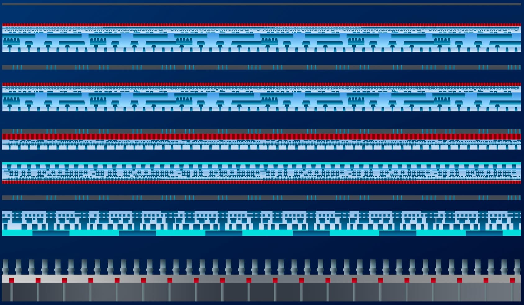
Figure 1 – Representation of a typical 3D NAND Flash structure (BL=bit line; WP=word plate; BSP=bottom select plate; SP=source plate; TSL=top select line).
State-of-the-art: gate-all-around vertical channels; up to 300 word-line layers
Although not pursued by all memory makers, the charge trap cell is the base of most 3D NAND structures today. This memory cell resembles a MOSFET transistor with the addition of a small layer of silicon nitride (SiN) inserted inside the transistor’s gate oxide (the oxide-nitride-oxide (ONO) stack). The SiN layer contains many charge-trapping sites that can hold an electrostatic charge. When the poly-Si gate is biased positively, electrons from the channel region tunnel through the oxide layer and get trapped in the SiN layer. This raises the threshold voltage of the transistor. The state of the cell can be measured by passing a voltage across the source/drain nodes. If current flows, the cell is in a ‘no-trapped-electrons’ state (corresponding to 1). Cells are in the ‘trapped-electrons’ (or 0) state if no current is measured.
The charge trap cell failed to be introduced in earlier 2D NAND planar configurations due to an insufficient memory window, which is measured as the difference in threshold voltage between program and erase. But in 3D NAND structures, this memory unit cell came to its full potential, thanks to a gate-all-around (GAA) vertical channel implementation method. In this GAA configuration, the gate stack completely wraps around the channel. This cylindrical geometry creates an enhanced field effect in the tunnel oxide. This leads to larger carrier injection into the trapping layers, enhancing the program/erase window.
The GAA fabrication typically starts with growing an oxide/word-line layer stack. Next, cylindrical holes are formed by drilling down through the stack using advanced dry etch tools. The tunneling (O) and trapping (SiN) layers and the poly-Si channel are then deposited along the sidewalls of the holes.
Recently, some major players announced the introduction of 3D-NAND-based products with up to 300 word-line layers stacked on top of each other, and this trend of increasing layers is expected to continue in the years to come. [1]
Ways to further increase bit storage densities
During the present decade, memory makers will push the conventional GAA NAND roadmap to its ultimate limits. Following the most optimistic projection, the number of layers will have increased to 1,000 by the end of the decade, accounting for 100Gbit/mm2 bit storage density [2]. This is, however, a slowdown of a few years with respect to the historical density scaling roadmap.
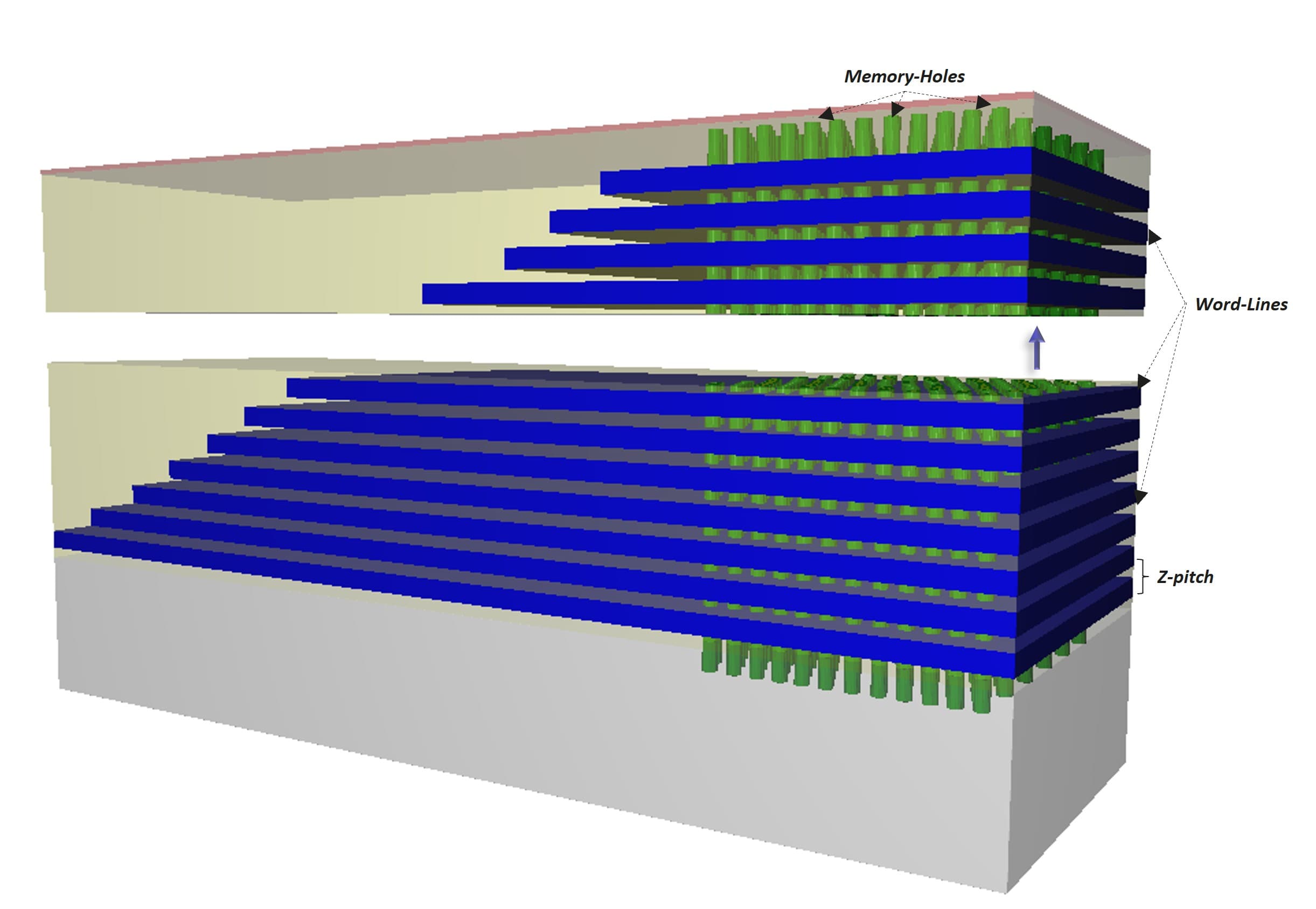
Increasing the number of layers introduces ever higher processing complexities and costs, challenges deposition and etch processes, and causes stress to build up inside the layers. To overcome these challenges, industry is introducing a few complementary process ‘tricks’ to obtain the 1,000 layers eventually. These include splitting the number of layers into two (or more) stacked tiers, further increasing the number of bits per cell, enhancing array efficiency, and reducing the GAA cell x-y pitch. There is also a trend to optimize the peripheral circuitry on a different wafer and attach it to the memory array using wafer-to-wafer bonding techniques. These innovations will, however, not be sufficient to control the growing processing costs, and therefore, an additional z-pitch scaling is pursued. Z-pitch scaling involves a reduction of the height of all materials involved in the layer stack, including word-line metals and oxides.
2030: introduction of the 3D trench cell architecture
In 2030, after GAA NAND Flash scaling has saturated, imec foresees the introduction of a new architecture to connect the charge trap cells: the trench cell architecture. With this architecture, 3D NAND moves away from the circular GAA memory cell geometry. Instead, the cells are implemented at the sidewall of a trench – resembling a planar configuration being tilted on its side – with two transistors at opposite walls of the trench. This next-generation NAND Flash cell architectures will not only offer the required leap in bit storage density; it is also believed to reduce costs. However, just like in the 2D planar configuration, the gate is no longer fully wrapped around the channel. Therefore, memory makers are concerned about an insufficient program/erase window.
Figure 2 – 3D schematics of (left) 3D NAND GAA and (right) trench devices (as presented at 2023 IMW).
Program and erase behavior of trench vs. GAA cell architectures
At the 2023 IEEE International Memory Workshop (2023 IMW), imec presented an experimental comparison of the memory operation of a trench cell with that of a GAA memory cell [3]. Both NAND Flash variants were processed on the same wafer, i.e., an in-house developed 3D NAND test vehicle with poly-Si gate and three word-line layers. Instead of cylindrical holes, trench features (300nm wide and 1µm long) were etched into the word-plane stack for the trench structure. Three vertical flat poly-Si channels (with 50nm – 200nm channel width) are formed along the sidewalls of the trench, and source/drain junctions are fabricated.
Without optimization, the trench cells do not perform as well as the GAA cells. They have non-ideal program and erase efficiencies, which are reflected in the slopes and onset of the incremental step pulse programming (ISPP) and erase (ISPE) curves, respectively. This translates into a smaller program/erase window. On the erase side, the ISPE curves also show a degradation in the erase saturation level.
Toward a 5V memory window
The poor memory window can be explained by the lack of a curvature-induced field effect, which, in the GAA case, increases the carrier injection into the trapping layer. To address this shortcoming, the imec team came up with an innovative solution, i.e., reducing the channel width of the trench device. Channel width scaling is expected to enlarge the impact of the curved high-injection regions formed around the edges of the channel. In other words, at a strongly reduced channel width, the trench cell starts to resemble a GAA cell from a geometrical point of view.
On the other hand, the degradation in the erase saturation level is mainly determined by parasitic electron injection from the gate. This can be suppressed by carefully engineering the gate stack and integrating a metal gate.
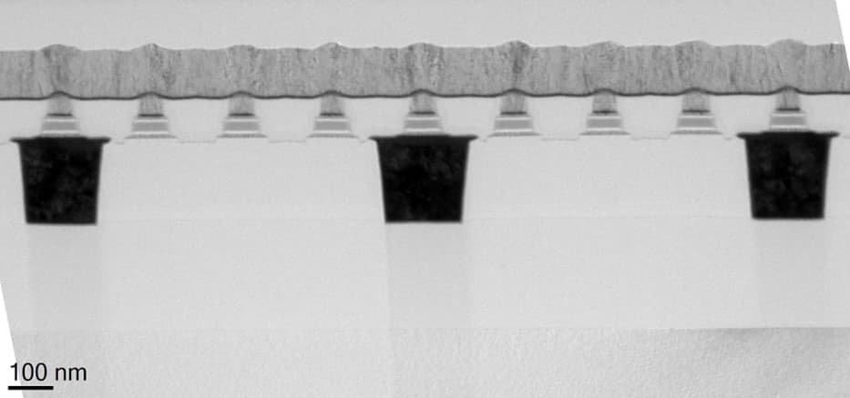
Imec showed experimentally that a better memory operation could be achieved for trench devices with scaled channel width (down to 30nm), combined with an alternative high-k liner material (such as ZrO2 or HfO2 instead of Al2O3), an engineered tunneling oxide and integration of a metal gate. For most of the studied conditions, a memory window as high as 5V was demonstrated, an improvement with 2V – without impacting retention and cycling behavior. The team is currently working on further improving the program and erase operation.
Figure 3 – (a) Trench channels at different channel width; (b) program and erase characteristics, showing an improvement at smaller channel width (as presented at 2023 IMW).
Ultrahigh bit storage density
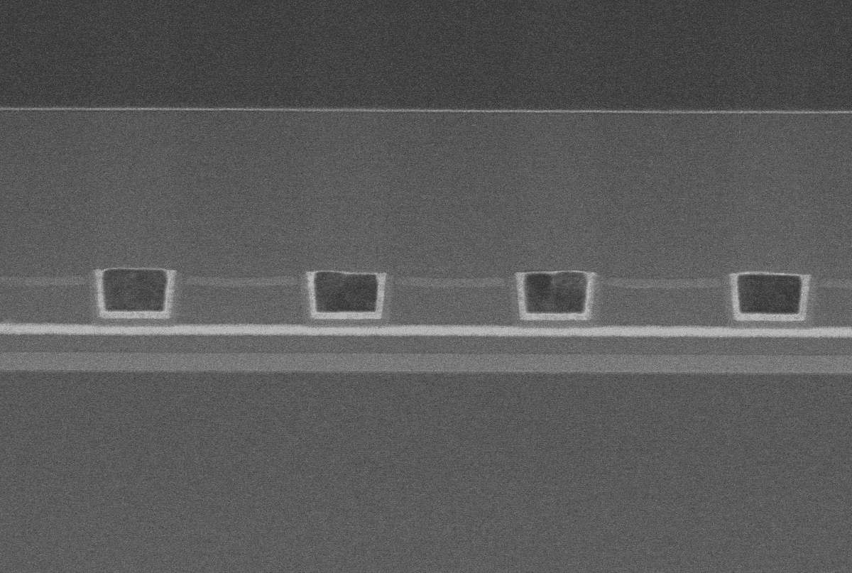
Having demonstrated a trench memory unit cell with good memory characteristics, the next step is to investigate potential industry-relevant integration schemes to stack a larger number of layers. Such a process flow is expected to resemble a GAA process flow, with the addition of an extra module: etching the vertical flat channel stripes at the side of the trench. Provided that a process solution can be found for this challenging etching step, imec proposed an emulation of a 3D trench process flow, with 220nm pitch trenches, each trench being 100nm wide and about 1µm long. To ensure high bit density, the flow is completed by etching 25nm wide channel stripes with an 80nm pitch.
Figure 4 – (a) Top view of the trench final design structure, and (b) cell density improvement factor of the trench architecture (as presented at 2023 IMW).
From the final design structure, the trench architecture is estimated to have a three times higher cell density than the GAA reference. This is expected to further improve with channel pitch scaling. Based on these results, the 3D trench architecture can be considered as a potential breakthrough for future 3D NAND Flash memories, with bit storage densities far exceeding 100Gb/mm2.
This article was originally published in eeWeb.
Want to know more?
[1] https://spectrum.ieee.org/flash-memory
[3] ‘Enabling 3D NAND trench cells for scaled Flash memories’, S. Rachidi et al., 2023 IEEE International Memory Workshop. Interesting in receiving the paper? Fill in our contact form.

Maarten Rosmeulen received his M.Sc. degree in physics in 1993 and his M.Sc. degree in physics of micro-electronics and materials science in 1994, both from the KU Leuven, Belgium. In 2005, he received his Ph.D. in electrical engineering from the KU Leuven. Since then, he has been with imec, in Leuven, Belgium, where he has been active as an R&D engineer in process integration, semiconductor device design, and electrical device characterization for multiple internal and external projects. In 2009 he became a project leader in developing GaN-on-Silicon Light Emitting Diodes (LEDs). In 2014 he became the team leader of the Pixel Design and Testing team and has been responsible for the development of CMOS Image Sensor (CIS) technologies. In 2019 he became the program director of the Storage Memory program, the position he holds today.
Published on:
7 June 2023


