Reliability of next-generation FETs with 2D material channels
Leuven | More than two weeks ago
Boosting reliability of 2D FETs for beyond-Silicon scaling
Background
2D materials like transition metal dichalcogenides are very promising to extend the logic scaling roadmap. Their atomically thin channel allows excellent electrostatic control and enable the ultimate device scaling. Many single-device demonstrators have been reported in literature, mainly highlighting the high performance during the initial electrical measurements. But upon repeated measurements, the performance typically degrades due to the high defectivity in the 2D channel (grain boundaries, point defects) and gate stack (adsorbates at interface, dangling bonds, oxide defects). To reach industrial adoption, fundamental understanding is needed about these defect types, their impact on the device performance and reliability, and to find ways to mitigate the degradation [1-2].
Key aspects of this PhD
- The impact of scaling and device morphology on electrical characteristics. The student will collect large datasets of electrical characteristics, understand the scaling trends and non-idealities by comparing with TCAD simulations, and develop new aging models that describe this new class of transistors.
- Investigate the impact of defects in the MX2 channel, gate stack and contacts on noise and reliability. The student will learn to use advanced measurement techniques like the Conductance technique on capacitors (C-V and G-V), Time-Dependent Defect Spectroscopy (TDDS), Random Telegraph Signal (RTS) and temperature-dependent noise measurements to investigate which factors influence the electrical impact of traps and their energy distribution. Additionally, the student will identify whether the hysteresis, bias temperature instability (BTI), and hot-carrier degradation (HCD) are driven by carrier capture in pre-existing electronic trap states, in newly created states, or by ionic diffusion.
- Possible defect candidates will be identified and incorporated into device and transport simulators, in collaboration with the ab initio and device modeling teams at imec, and fed back to further improve device processing.
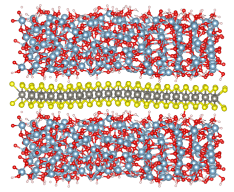
The 2D FETs are fabricated using a state-of-the-art 300mm fab-based fabrication flow for double-gated MX2 devices (e.g. WS2 and MoS2) [3-4]. The student will work closely with process, integration and device engineers to apply findings and improve the device characteristics over several fabrication cycles. The student will build upon expertise already accumulated within the reliability team [5-7].
[1] Lanza, M., Smets, Q., Huyghebaert, C., & Li, L.-J. (2020). Yield, variability, reliability, and stability of two-dimensional materials based solid-state electronic devices. Nature Communications, 11(1), 5689. https://doi.org/10.1038/s41467-020-19053-9
[2] Illarionov, Y. Y., Rzepa, G., Waltl, M., Knobloch, T., Grill, A., Furchi, M. M., Mueller, T., & Grasser, T. (2016). The role of charge trapping in MoS 2 /SiO 2 and MoS 2 /hBN field-effect transistors. 2D Materials, 3(3), 035004. https://doi.org/10.1088/2053-1583/3/3/035004
[3] Asselberghs, I., Smets, Q., Schram, T., Groven, B., Verreck, D., Afzalian, A., … Radu, I. P. (2020). Wafer-scale integration of double gated WS 2 -transistors in 300mm Si CMOS fab. In 2020 IEEE International Electron Devices Meeting (IEDM) (pp. 40.2.1-40.2.4). IEEE. https://doi.org/10.1109/IEDM13553.2020.9371926
[4] Schram, T., Sutar, S., Radu, I., & Asselberghs, I. (2022). Challenges of Wafer‐Scale Integration of 2D Semiconductors for High‐Performance Transistor Circuits. Advanced Materials, 34(48). https://doi.org/10.1002/adma.202109796
[5] Panarella, L., Smets, Q., Verreck, D., Schram, T., Cott, D., Asselberghs, I., Kaczer, B. (2022). Analysis of BTI in 300 mm integrated dual-gate WS2 FETs, In 2022 Device Research Conference (DRC) (pp. 1-2). IEEE. doi: 10.1109/DRC55272.2022.9855819
[6] Panarella, L., Kaczer, B., Smets, Q., Verreck, D., Schram, T., Cott, D., Asselberghs, I., ..., Afanas’ev, V. (2023). Impact of gate stack processing on the hysteresis of 300 mm integrated WS2 FETs. In 2023 IEEE International Reliability Physics Symposium (IRPS) (pp. 1-6). IEEE. doi: 10.1109/IRPS48203.2023.10117803
[7] Panarella, L., Kaczer, B., Smets, Q. et al. Evidence of contact-induced variability in industrially-fabricated highly-scaled MoS2 FETs. npj 2D Mater Appl 8, 44 (2024). https://doi.org/10.1038/s41699-024-00482-9
Required background: solid-state physics, semiconductor physics, semiconductor devices, electrical circuits, physical and electrical characterization techniques
Type of work: 15% theory, 15% modeling and simulation, 70% experimental work
Supervisor: Michel Houssa
Co-supervisor: Valeri Afanasiev
Daily advisor: Ben Kaczer, Quentin Smets
The reference code for this position is 2025-051. Mention this reference code on your application form.