Exploring area-selective deposition with new materials for fabricating smaller, faster and more energy efficient electronic devices
PhD - Leuven | More than two weeks ago
Today, electronic devices are omnipresent in our society and they affect important sectors such as communication, healthcare, transport, energy, education, and research and development. The wide availability of computing power and memory is the result of a spectacular evolution from planar micro-electronic devices to 3D nano-electronic devices. Further innovations target realizing smaller and faster electronic devices that are more energy-efficient. At the same time, we are committed to improve the environmental impact of electronic device fabrication [1].
Traditional electronic device fabrication is based on top-down patterning by deposition, lithography and etching. Materials are deposited everywhere on a substrate and nanopatterns are created by removing the material where it is not needed. Lithography is an established technique that has been used for decades, and it has enabled scaling to the nanometer scale. However, as dimensions decrease, it becomes more and more difficult to align patterns that are created by subsequent lithography steps, and the misalignment errors have more detrimental impact on device performance.
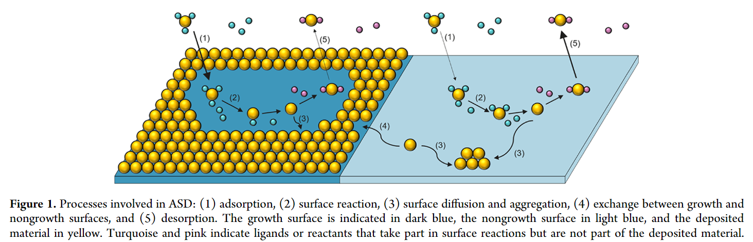
A promising future direction is to combine conventional top-down patterning techniques with emerging bottom-up strategies like area-selective deposition (ASD). ASD is a technique to deposit material only where needed, on a given area of a patterned substrate and not on adjacent surface area. As such, a given pattern is replicated. ASD has great potential to improve the fabrication processes for nano-electronic devices [2]. Another benefit is that ASD requires fewer chemical products and less energy as compared to the traditional top-down patterning processes.
This PhD project will explore new ASD processes and their applications in nanopatterning:
- We will investigate the fundamental mechanisms during ASD of dielectrics and metals on nanopatterns with materials relevant for the nano-electronic devices of the future, including 2D materials (MoS2, WS2, …) and novel resist materials. The aim is to gain insight into the chemical and physical processes during ASD by chemical vapor deposition and atomic layer deposition, facilitating rational ASD process design [4].
- In a next phase, we will explore the potential applications of the resulting ASD process in nanopatterning, for example by using the ASD grown material as a hard mask for pattern transfer to advanced material stacks.
You will be part of the Nano-engineered Thin Films (kuleuven.be) research group located at imec. As such, you benefit from our vast experience on thin film deposition [3,4] and the state-of-the-art research infrastructure of the imec clean room and associated characterization labs. You will enrich your competences through the PhD trajectory at the KU Leuven and the imec academy development center. You will share your insights with imec’s industrial partners and with the international research communities through conferences and publications.
[1] Imec's chip scaling roadmap: smaller, better, faster | imec (imec-int.com)
[2] G. N. Parsons and R. D. Clark, Chem. Mater. 32, 4920 (2020)
[3] F. Grillo, J. Soethoudt, E. A. Marquez, L. de Martin, K. Van Dongen, J. Ruud van Ommen, A. Delabie, Area-selective deposition of ruthenium by area-dependent surface diffusion, Chem. Mater. 32, 9560 (2020).
[4] I. Kandybka, B. Groven, M.H. Silva, S. Sergeant, A.N. Mehta, S. Koylan, Y. Shi, S. Banerjee, P. Morin, A. Delabie, Chemical vapor deposition of a single-crystalline MoS2 monolayer through anisotropic 2D crystal growth on stepped sapphire surface. ACS nano, 18, 3173, (2024).
Required background: Chemistry, material science
Type of work: 70% experimental, 20% modelling, 10% literature
Supervisor: Annelies Delabie
Daily advisor: Pierre Morin
The reference code for this position is 2025-027. Mention this reference code on your application form.
![]()