Metrology-informed TCAD simulation of process variability in NanoSheet-based transistors
Master projects/internships - Leuven | Just now
Combining metrology and simulation to assess how process variability shapes the performance of nanosheet transistors in next-generation semiconductor nodes.
The semiconductor industry relies on transistor scaling to satisfy the computing demands of emerging AI, cloud and mobile applications. Transistor scaling beyond the current 3nm logic node involves switching to Nanosheet-based Gate All-Around (GAA) transistor architectures [1]. The fabrication process of this new generation of devices involves hundreds of processing steps that require nanometer scale precision. At these dimensions, the variability of processes as well as the intrinsic variability of the properties of the materials critically impact the devices’ performance and reliability [2]. For this reason, correlating process variations to device properties and device metrics is now more important than ever to individuate the most critical process steps and allow for effective device development.
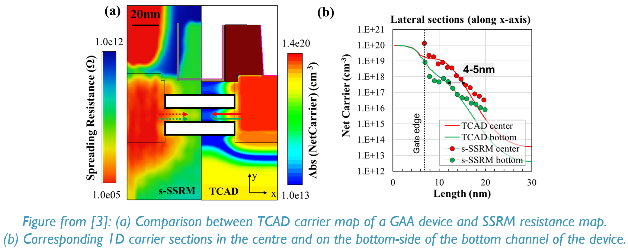
The candidate will combine various metrology and electrical data with Technology Computer Aided Design (TCAD) simulations to individuate and measure different process variations and simulate their impact on key device performance metrics [3]. The student will determine how to translate dimensional information from imaging techniques such as Transmission Electron Microscopy (TEM) and Atomic Force Microscopy (AFM) into statistically valid morphology variations of the devices being simulated. Compositional analysis such as Secondary Ion Mass Spectroscopy (SIMS) and Energy-dispersive X-ray spectroscopy (EDS) will be used to quantify the variations between different processes and their impact on dopant concentrations or gate-stack layers compositions. These are important modules closely related to device access resistance and threshold voltage. The candidate then will be responsible for correlating such experimental data with the anticipated impacts and, ultimately, using simulations to assess the effects on device properties. Finally, with the use of Scanning Spreading Resistance Microscopy (SSRM) data, the candidate will be able to extract the variability in junction engineering and use this information for the evaluation of the role of carrier distribution on device performance.
This project aims to establish a comprehensive framework for correlating process variability to device performance not only using conventional TCAD simulations, but by introducing a sophisticated approach that involves the additional use of metrology data. The candidate will gain a detailed understanding of cutting-edge semiconductor processing, process and device simulations, and advanced metrology techniques. The insights generated through this work will be valuable for the development of next-generation logic nodes and semiconductor technology.
[1] N. Horiguchi et al., “CMOS Scaling by Nanosheet Device Architectures and Backside Engineering,” in 2024 International VLSI Symposium on Technology, Systems and Applications (VLSI TSA), IEEE, 2024.
[2] X. Yang et al., “Impact of Process Variation on Nanosheet Gate-All-Around Complementary FET (CFET),” IEEE Trans Electron Devices, IEEE, 2022.
[3] P. Eyben et al., “Combining TCAD and advanced metrology techniques to support device integration towards N3,” in 2021 20th International Workshop on Junction Technology (IWJT), IEEE, 2021.
Type of Project: Internship; Combination of internship and thesis
Master's degree: Master of Engineering Science; Master of Science
Master program: Nanoscience & Nanotechnology; Physics; Electrotechnics/Electrical Engineering
Duration: 4 - 6 months
Supervisor: Anne Verhulst (ESAT)
For more information or application, please contact the supervising scientists Pierre Eyben (Pierre.Eyben@imec.be), Andrea Pondini (Andrea.Pondini@imec.be) and Philippe Matagne (Philippe.Matagne@imec.be).
Imec allowance will be provided for students studying at a non-Belgian university.
![]()