Bias Temperature Instabilities of Replacement Metal Gate stacks for Advanced Logic Devices beyond the 2nm CMOS node
Leuven | More than two weeks ago
Reliability characterization and physics-based modeling to enable the next generation CMOS tech
To support the unabated performance enhancement of CMOS technology, which fuels innovation of all fields of our society, the MOSFET device architecture has reached extraordinary degrees of scaling and complexity. A decade ago industry moved from the classic planar transistor to finFET architectures, and it currently prepares to switch to the even more complex NanoSheet structure. For beyond that, novel concepts to minimize the footprint of a single logic gate (an nMOS and a pMOS transistor combined) are currently being explored, including the ForkSheets (lateral co-integration) and the CFETs (vertical stacking). Each subsequent device technology must offer enhanced performance while guaranteeing sufficient reliability.
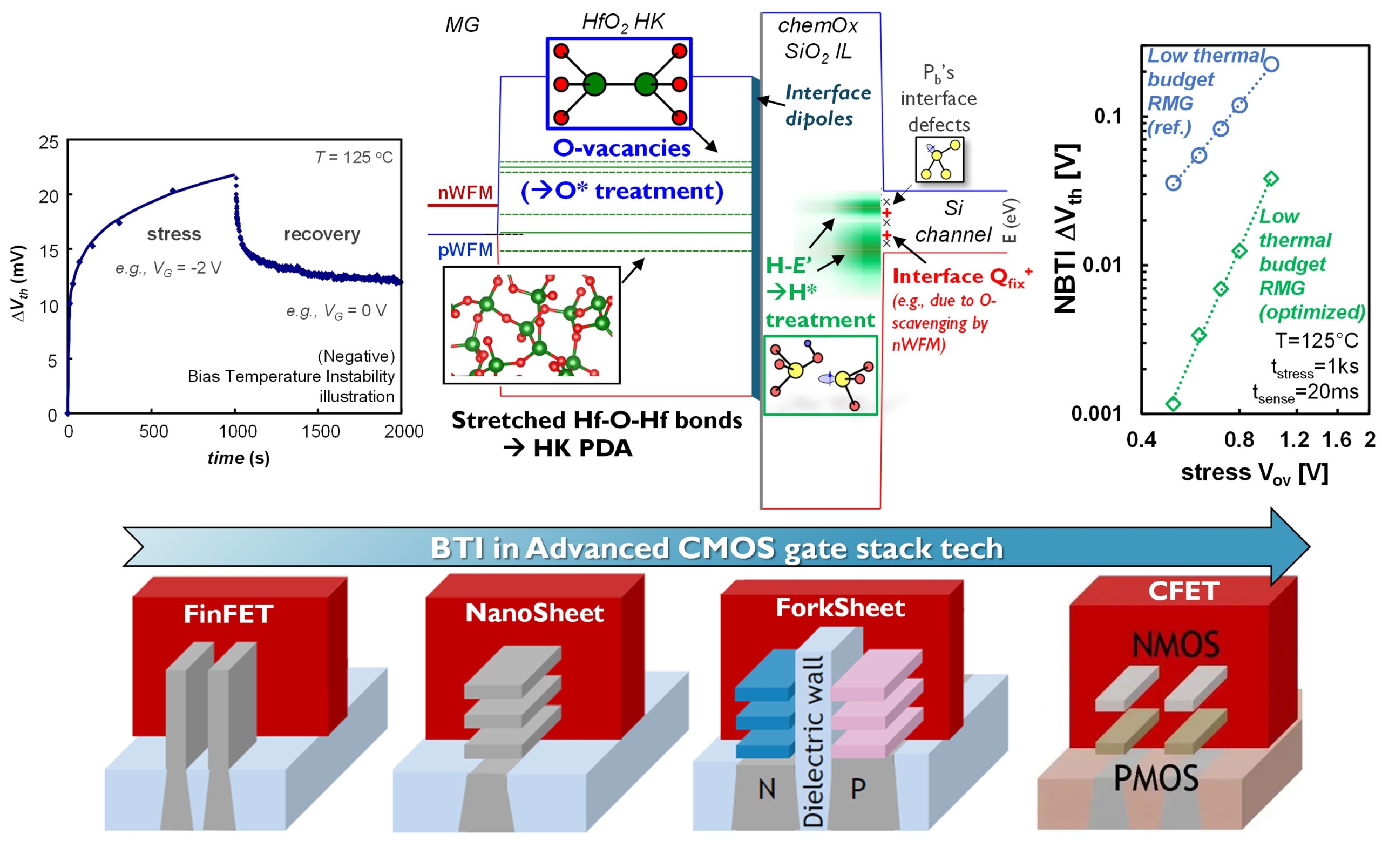
Bias Temperature Instabilities (BTI) are the primary reliability concern in CMOS technologies. The charging and discharging of pre-existing dielectric defects, and the generation of additional defects during device operation induce a gradual drift of the device electrical metrics which can yield to circuit performance loss and potentially to circuit failure.
The gate dielectric technology has been advanced substantially in recent years. After the introduction of high-k dielectrics, which replaced the native Si oxide ~15 years ago, the gate stack fabrication flow has moved from the traditional “Gate-First” integration to the so-called “Gate-Last” or “Replacement Gate” integration, where a dummy gate stack used for the self-aligned source/drain fabrication is replaced by the final high-k dielectric only towards the end of the fabrication flow. In this scheme, the gate dielectric is not exposed to the high temperature anneals required for channel doping activation—this approach thus enables the usage of different metals (even some with limited thermal stability) as gate electrodes to control the transistor threshold voltage (Vth) but requires dedicated anneals to cure dielectric defects after deposition. Recently, progress has been made on the identification of the microscopic defect structures present in the dielectric stack, and suitable cures for each of them have been developed on conventional planar device test vehicles. Such novel solutions need to be validated on and optimized for future transistor architectures.
Furthermore, in current CMOS technology nodes, multiple transistor flavors with different threshold voltages are offered for flexible System on Chip (SoC) design, e.g., low Vth transistors for high performance circuits and high Vth transistors when low power consumption is the priority.
In advanced transistor structures, Vth controls is obtained by deploying different gate metals or by inducing the formation of dipoles across the dielectric stack by depositing rare-earth based interlayers. This approach introduces a variety of species in the dielectric stack, and thus can impact the gate stack stability and reliability. Furthermore, it can affect also the device-to-device variability across wafer, due to e.g., non-uniform layer depositions or localized charged defect formation.
The plethora of novel gate stack configurations currently available (various metal stacks, various dipole-forming interlayers, various treatments, different channel polarity, various device architectures) calls for a continuous fundamental assessment of BTI.
This PhD study will focus on:
- Experimental characterization of BTI in advanced gate stacks for both nMOS and pMOS devices, with different gate metals, dipole-inducing interlayers, and dielectric treatments, utilizing first simplified test vehicles (e.g., capacitors and planar transistors);
- Validation and optimization of novel gate stack solutions on advanced device test vehicles (e.g., nanosheets and CFETs);
- Reliability and variability benchmarking and physics-based interpretation.
The PhD candidate will be embedded in the Device Reliability and Electrical (DRE) characterization team of imec, which has a strong expertise in reliability characterization and modeling and established characterization labs to support this study.
Required background: Semiconductor Physics (MSc in Electrical Engineering/Physics or equivalent); Valuable assets: experience with transistor-level electrical measurements, statistical data analysis, TCAD simulations, programming skills (Python, SciPy or Matlab or equivalent)
Type of work: 50% electrical characterization, 20% data analysis, 20% modeling, 10% literature
Supervisor: Michel Houssa
Co-supervisor: Jacopo Franco
Daily advisor: Jacopo Franco
The reference code for this position is 2025-041. Mention this reference code on your application form.