Eric Beyne, imec fellow & program director 3D system integration
2017 saw a clear breakthrough for 3D chip technology in commercial products. Before then, the industry had looked rather skeptically at 3D, but now it is beginning to realize that 3D does not necessarily have to cost more money. Better still, it creates new possibilities and opportunities.
3D on the market
In 2017 we saw 3D chip technology start to appear in a range of different commercial products. For example, the iPhone 8 features Sony’s ‘stacked’ image sensor. This sensor delivers a unique picture quality for both photos and videos because the image sensor, computing chip and memory have all been stacked together to create a single unit. 3D is also the way to go for memory. Consider, for instance, the growing use of high-bandwidth modules. These modules contain 4 or 8 DRAM memory chips stacked on top of a processor chip. In 2017 both AMD and Nvidia released powerful processors onto the market based on this principle. These processors can be used in high-end laptops, as well as for applications connected with artificial intelligence.
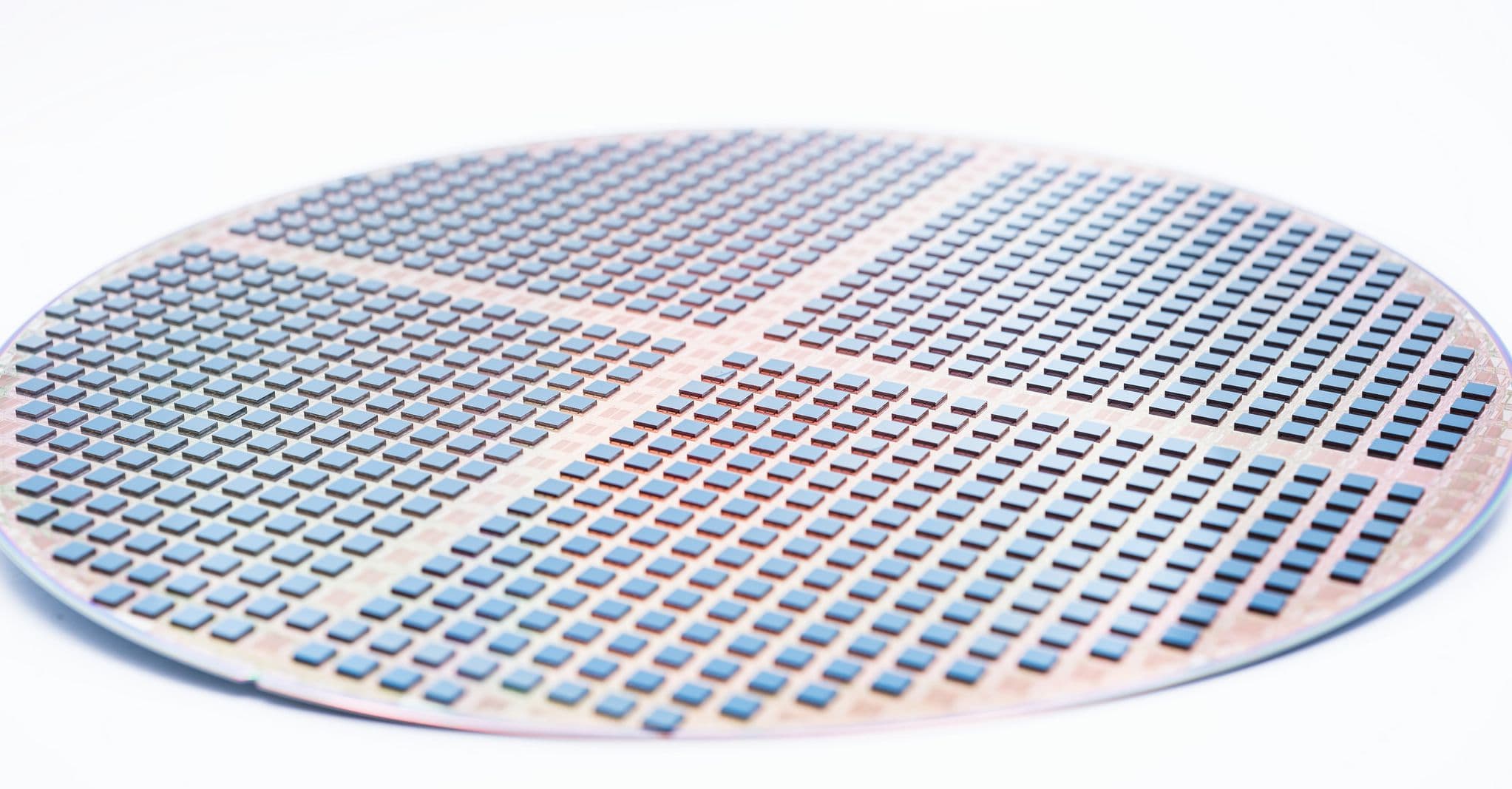
2017 also provided a tremendous boost for “fan-out wafer-level packaging” technology (WLP). Fan-out WLP should be considered as a logical next step following standard WLP, tackling the problem of the growing mismatch and interconnect gap between chips and printed circuit board. The chips are sliced out of a silicon wafer and transferred to a carrier-wafer, where they are positioned further apart than on their original wafer. The reconstructed wafer is then coated with an epoxy mold compound, a redistribution layer and solder balls. The technology was developed around 15 years ago by Infineon, but is currently going through a real revival as an effective way of stacking wafers on top of each other. The Apple A10 processor, for example, uses TSMC’s fan-out technology, called inFO, to stack the DRAM memory and the CPU.
The most suitable technology for every building block
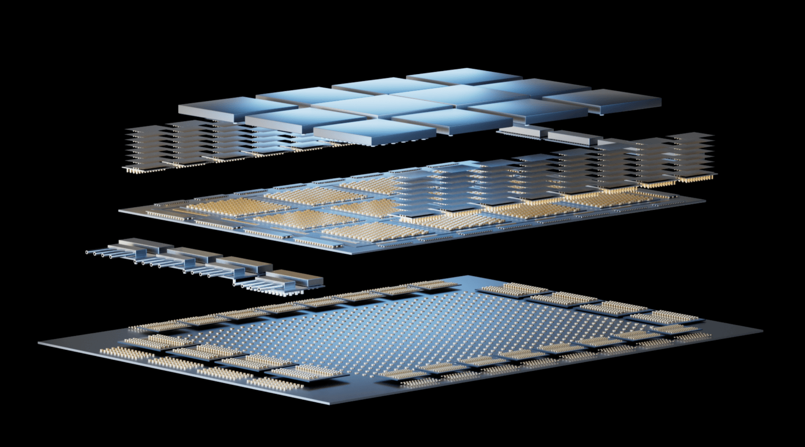
Over the coming years we will see 3D chip technology appear increasingly in a very wide variety of applications, especially where those applications require a great deal of computing power and memory capacity. These uses will include multi-core servers and applications related to artificial intelligence. Systems will also become increasingly ‘heterogeneous’, which means that 3D technology is essential. A heterogeneous system is made up of various specialized components, such as memories, image sensors, III-V electronics for analog functions and RF, processors, low-power electronics, etc. By designing and processing each of these components separately with the most appropriate technology and then packaging them all into a single unit using 3D technology, we will be able to make even more progress in terms of performance, cost and power consumption of electronic systems.
Wafer-to-wafer bonding
At imec we have long believed in the power of 3D technology and we are devoting a great deal of energy into improving it. In 2017, for example, we achieved excellent results with wafer-to-wafer bonding. During the year, we succeeded in further reducing the distance between the chip connections (pitch) in hybrid wafer-to-wafer bonding to 1.4 micrometer (the current standard pitch in the industry is 6 micrometer). We believe that a pitch of 0.7 micrometer should be achievable for 2018. This research is linked closely with the work of the 3D equipment suppliers that are part of our 3D program.
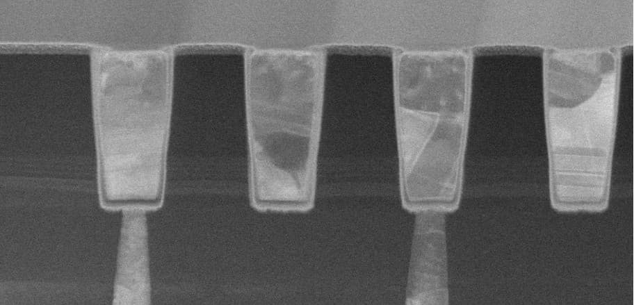
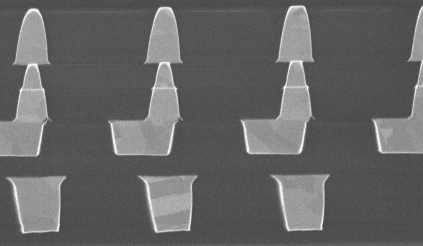
Again in 2017, in the area of wafer-to-wafer bonding, but this time in via-last technology, we managed to reduce the diameter of the through-silicon via to 1 micrometer, with a pitch of 2 micrometer (the current standard in the industry is a 5 micrometer diameter and a 10 micrometer pitch). In 2018 we will further expand our optimized technology to include the stacking of 4, 8 and 16 wafers. The stacking of so many wafers is particularly important for memory applications.
For die-to-wafer technology we have been able to achieve a microbump pitch of 10 micrometer at the moment. In 2017, the focus was on developing collective bonding techniques so that the die-to-wafer process can be carried out faster and at a lower cost. In current die-to-wafer processes the chips are still transferred one by one. With collective bonding, on the other hand, the chips are placed on a carrier-wafer and transferred together to another wafer for bonding. In 2017, we developed a concept flow for this process and demonstrated its feasibility for industry. We also ensured that the process can now be used to transfer non-silicon chips onto silicon wafers (such as optical I/O, lasers, III-V, power amplifiers, microLEDs, etc.). This expansion of the technology is important for the future, because we will be dealing increasingly with heterogeneous systems that consist of specialized components.
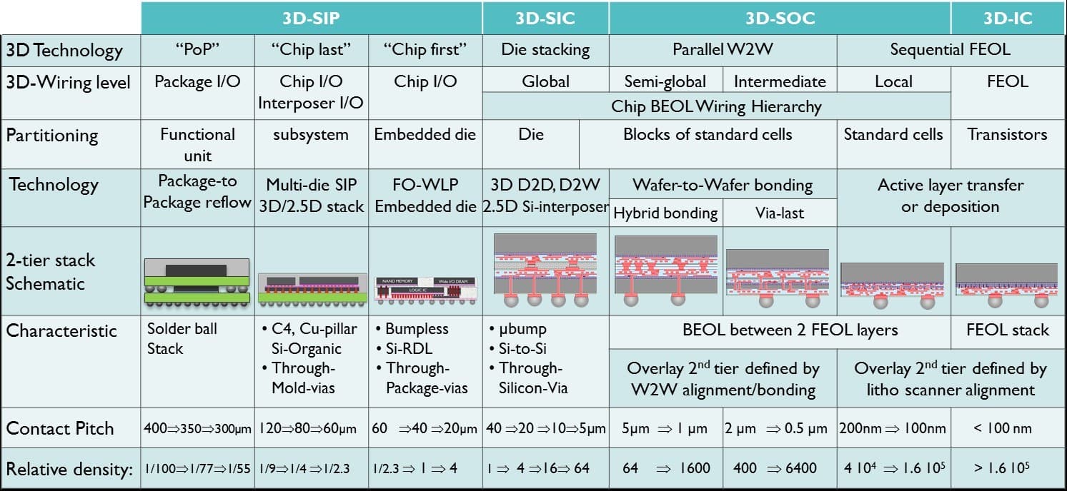
Imec’s 3D technology landscape. We prefer not to talk about a ‘roadmap’ because for 3D there will be many options working alongside each other, even within a single system.
Cooling chips with microjets
The most innovative road that we went down in 2017 is very definitely the use of 3D prototyping for chip packages and more specifically in developing a new concept for chip cooling.

Now that the resolution of 3D prototyping is improving all the time, it will be interesting to apply this technology for electronic systems.
It will then be possible to optimize the design of the chip packaging specifically for the application, instead of using a standard design (also here, you have a trend toward specialization). 3D prototyping appears to be the perfect way of converting our chip-cooling concept into reality. The concept consists of putting microfluidic layers on the rear side of the chip, which then direct tiny microjets onto the chip and in doing so disperse the heat very efficiently. The performance – and cost! – of this cooling system is also far better than the current state-of-the-art process. This is the case in particular because various intermediate layers can be left out and the rear side of the chip can be cooled directly.
In 2018 we will develop this technology further, based on 3D printing. This will enable us to optimize the design and take it in a direction that is not possible with conventional production technologies. These advances will include the completion and 3D design of supply channels in order to avoid unnecessary drops in pressure (= losses). Hence we will be able to get the coolant onto the surface in the best possible way.
Want to know more?
- Want to know more about the new concept for cooling chips? Then click here to retrieve the IEDM paper by Herman Oprins et al.
- Read the article about 3D systems-on-chip published in the April 2017 edition of imec magazine.
Eric Beyne obtained a degree in electrical engineering in 1983 and a Ph.D. in Applied Sciences in 1990, both from the Katholieke Universiteit Leuven, Belgium. Since 1986 he has been with imec in Leuven, Belgium where he has worked on advanced packaging and interconnect technologies. Currently, he is an imec fellow and program director of imec’s 3D System Integration program.
Published on:
15 December 2017


