Intro
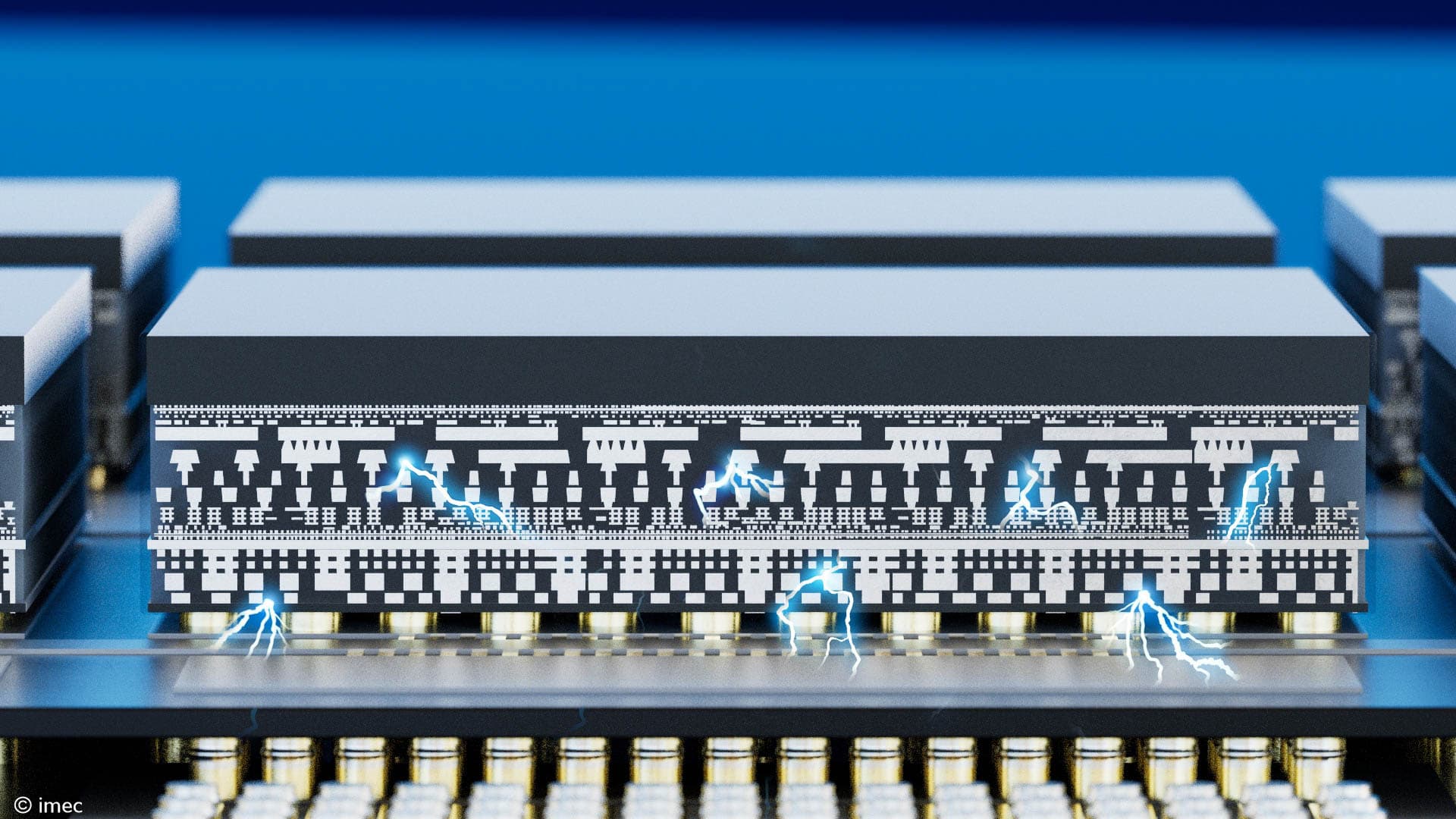
3D chips enable high-performance and cost-effective systems. But, as is the case with every new technology, it comes with new reliability and failure issues.
One of these are faults – electrical opens and shorts – in through-silicon vias (TSVs) that interconnect the stacked chips. Researchers at imec have now developed a new technique that can rapidly localize these interconnection failures in a non-destructive and cost-effective manner at wafer scale.
Postdoctoral researcher Kristof J.P. Jacobs sheds light on the new technique and unveils first results on a second – related – technique which allows chips to be investigated at an even deeper level.
Through-silicon vias form the heart of 3D chips
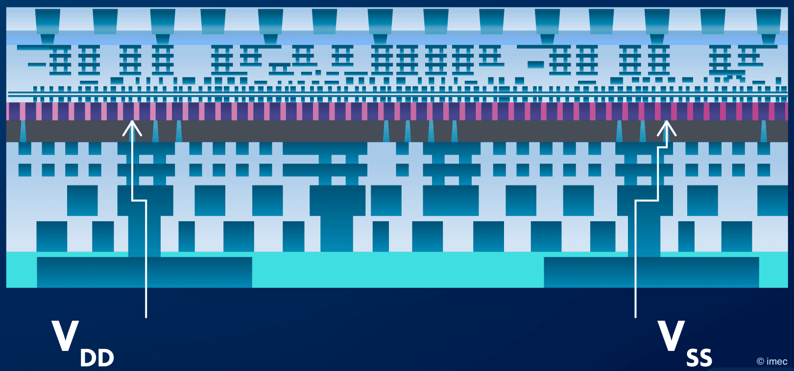
Stacking chips on top of each other is a well-known approach to make small high-performance systems, with the possibility to combine different technologies for each layer in the system. 3D chips are used in high-bandwidth handheld products and high-density multi-chip memory. At the heart of the 3D chips are through-silicon vias (TSVs) which provide the shortest chip-to-chip interconnects and the smallest pad size and pitch. The fabrication of these TSVs is a challenge, involving processes such as deep Si etch, chemical vapor deposition (CVD) oxide insulation, metal barrier & seed deposition, copper electroplating and chemical mechanical polishing (CMP).
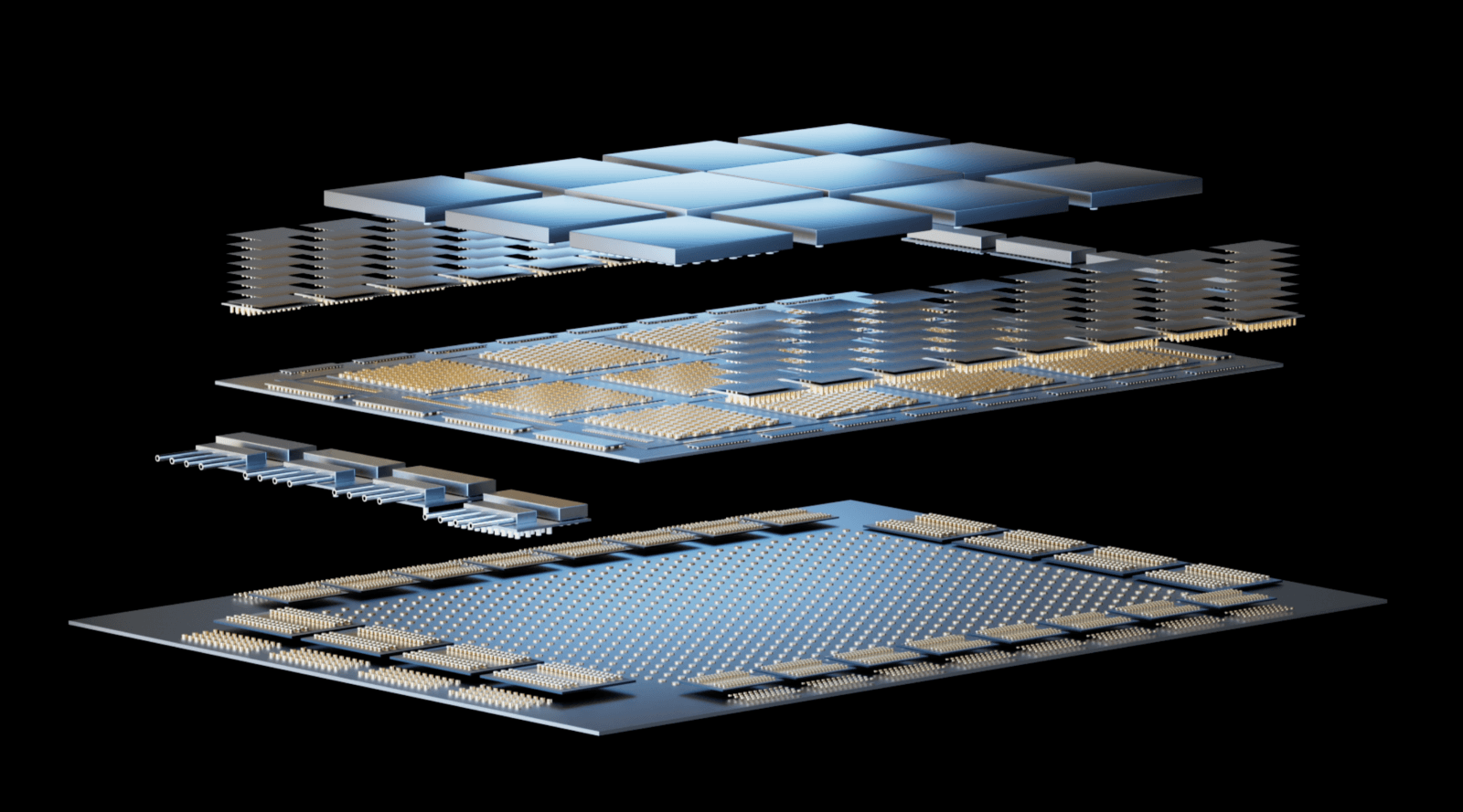
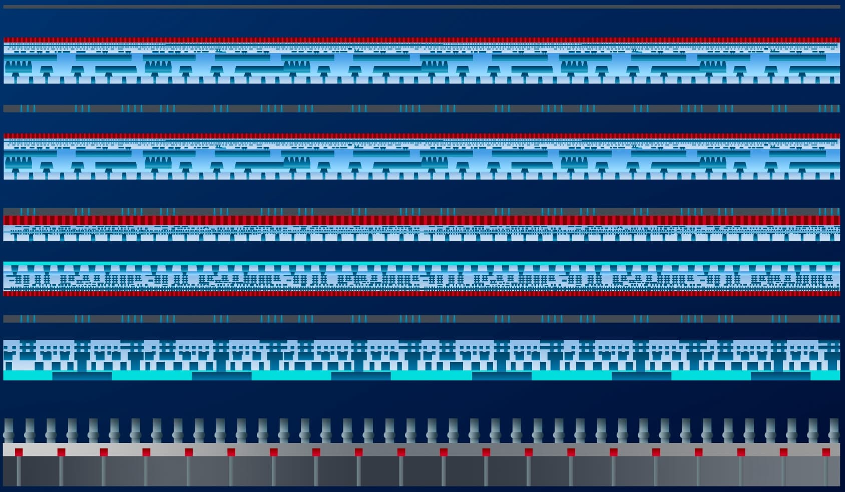
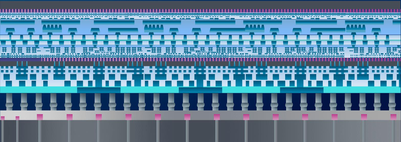
Stacking chips using 3D heterogeneous integration
These 3D specific processes and operations bring new reliability issues and failure mechanisms that require new failure analysis (FA) methodologies as traditional methods are becoming impractical for today’s IC complexity. FA forms an important function for chip manufacturing as it provides valuable information for technology advancement and corrective action for quality and reliability improvement.
Today, only a limited number of non-destructive techniques are available to localize interconnection failures in 3-D chips. The most promising techniques include magnetic field imaging (MFI), lock-in thermography (LIT), and electro optical terahertz pulse reflectometry (EOPTR). Whilst each of these techniques has unique characteristics and advantages (as well as limitations), they all require highly specialized and expensive FA apparatus that is not available in many laboratories.
To address the need for rapid, cost-effective, and scalable FA techniques, imec has developed a new method to localize interconnection failures in 3-D chips. This technique, called LICA, exploits the effect of light on TSV capacitance for defect localization. Moreover, it only requires a scanning laser microscope, probing station, and capacitance meter which are all readily available lab tools.

Through-silicon vias are at the heart of 3D chips. TSV failure analysis is indispensable to optimize the production of 3D chips.
LICA – Defect localization with light waves

LICA stands for light-induced capacitance alteration. It refers to the fact that the electrical capacitance of the TSV changes when it is illuminated with light (photocapacitance).
However, when a fault is present in the TSV, and the light shines at this position, no change in capacitance will be detected as the electrical connection to the meter is interrupted. This way, the fault can be localized. The technique builds on the capacitance-voltage (C-V) measurement method, yet also allows to conduct the measurement on a local level. Unlike scanning capacitance microscopy (SCM), whereby the local capacitance is measured between the sample and a small tip that is scanned over the surface, a focused laser beam is used to induce a change in the TSV capacitance.
The photosensitivity of the TSV capacitance depends on many factors such as light wavelength and measurement frequency. Imec researchers investigated the effects of these factors to determine the optimal measurement conditions for maximum signal strength. It was found that up to ~70% of the TSV capacitance can be made sensitive to light under optimal conditions. As the signal is typically in the range of a few tens of femtofarads (10-15 F), commercially available capacitance meters can be used for the detection. While the sensitivity of commercial meters may be sufficient for single die measurements, the associated measurement time is considered too long for wafer level defect screening. To address this, imec developed an ultra-sensitive measurement instrument that further reduces the measurement time from hours to minutes.

With LICA, the light-induced change in electrical capacitance is measured while scanning a focused laser beam over the 3D TSV structure under test. Test probes provide electrical connections from the structure to the measuring instrument. The location of the defect is marked when a distinctive change in the capacitance response is detected.
Technology demonstration
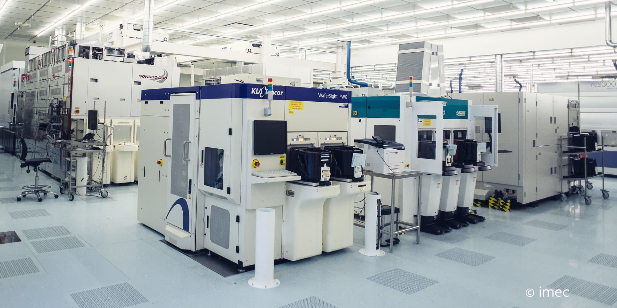
The technique has been demonstrated on a 5x50 µm via-middle TSV chain structure fabricated in imec’s state-of-the art 300mm cleanroom. The purpose of a TSV chain structure is to evaluate the electrical continuity of multiple TSVs connected in a chain configuration. Measuring the chain resistance may indicate whether the structure is yielding or not, but it provides no information on the location of the defect. Accurate defect localization is required to understand the cause of the failure.
To demonstrate the applicability of the LICA technique, an open failed TSV structure was selected which includes over 650 TSVs with a TSV pitch of 20 µm.
By scanning the focused laser beam over the chain, and applying a differential capacitance measurement technique, imec researchers have been able to successfully localize the open defect in the structure down to a single TSV. The required measurement time to localize the defect was less than five minutes. We expect that the analysis time can further be reduced to less than one minute by instrumentation optimization. Today, the LICA technique is used within imec to assist in the development of 3D integration technologies.

The pass/fail wafer map shows the location of the die failures but contains no information on the exact failure location in the structure. With LICA, failures can be localized more accurately down to a single TSV.
Future work: thermal technique for stacked chips
A limitation of the LICA technique is that the region of interest should be accessible by the laser. Unlike dielectric passivation – which can be transparent to the light – metal layers, underfill, and epoxy overmold can block the path of the light.
This can be a problem when stacked chips are being investigated and the faults are in the middle or bottom chips. That’s why the imec research team is currently developing a second – similar – technique based on thermal waves (instead of light waves) which have the ability to penetrate through these materials. This technique will enable defect localization regardless of whether the defect is in the top or bottom die.
Want to know more?
If you would like to receive the technical paper on this subject, entitled “Light-induced capacitance alteration for non-destructive fault isolation in TSV structures for 3D integration”, please send an email to imecmagazine@imec.be.

Kristof J.P. Jacobs is a postdoctoral research fellow from KU Leuven at imec. He is part of the reliability group where his research focuses on failure analysis for 3-D technologies. His other research interests include semiconductor material/device characterization and terahertz (THz) technology. He holds a MSc in Electronic Engineering and a PhD in Semiconductor Photonics from the University of Sheffield, UK.
His thesis research was conducted on the manufacturability of high current density resonant tunnelling diodes for THz technologies. During his doctorate, he developed new growth, process, and characterization technologies for the realization of compact THz sources in partnership with Rohm Semiconductor, Japan.
Published on:
5 September 2017


