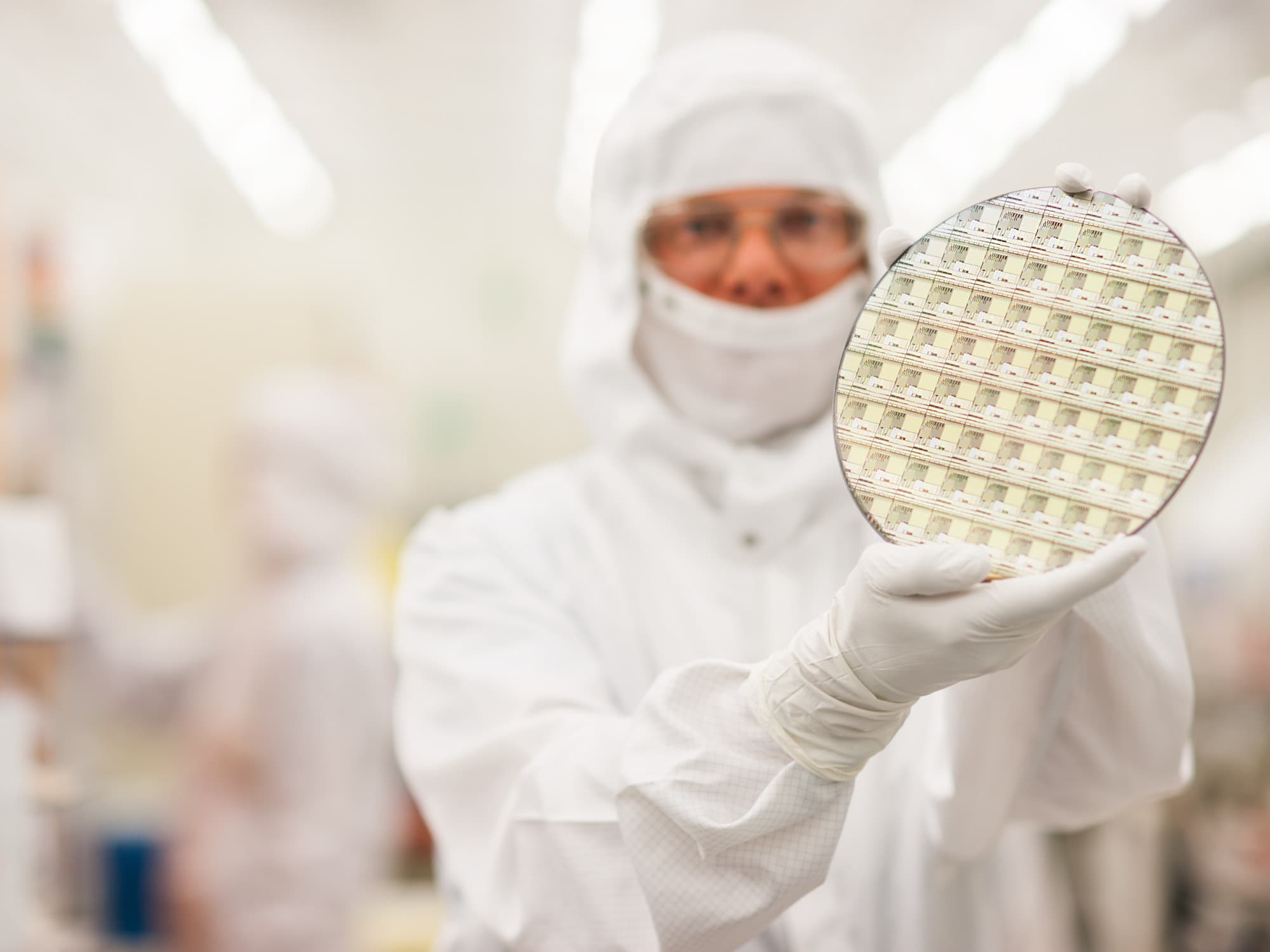
Gallium-nitride-on-silicon (GaN-on-Si) technology is maturing at a rapid pace and is expected to be adopted soon in different markets. Applications mainly include high-voltage power switching and power conversion, RF power amplifying and sensing. But for certain applications, the technology has a considerable disadvantage: multiple GaN devices (such as high electron mobility transistors) have limited capability for monolithic integration on the same GaN-on-Si wafer. Imec researchers therefore take a different approach and combine, for the first time ever, GaN-on-SOI (silicon on insulator) technology with trench isolation to achieve monolithic integration. They presented their results at the 2017 Workshop on Compound Semiconductor Devices and Integrated Circuits (WOCSDICE) and the work has been published in IEEE Electron Device Letters.
GaN-based power devices
GaN is anticipated to be the next generation power semiconductor. With a higher breakdown strength, faster switching speed, higher thermal conductivity and lower on-resistance, power devices based on this wide-bandgap semiconductor material can significantly outperform the traditional Si-based power chips. Initially, the development of GaN-based technology focused on high-voltage (600V) power-switching applications and lower-voltage DC-DC converters. As such, the first-generation GaN-based power devices will play a key role in the power conversion within battery chargers, smartphones, computers, servers, automotive, lighting systems and photovoltaics. Meanwhile, new opportunities in other application areas are emerging, including RF power amplifiers for future 5G wireless communication and GaN-based gas- and biosensors.
In absence of viable low-cost GaN bulk substrates, GaN is grown on a variety of substrates, the most popular being sapphire, silicon carbide (SiC) and Si. Si substrates have become attractive for GaN growth because of their larger wafer diameter (200mm and higher) and lower cost perspective, and the ability to use standard semiconductor processing lines.
The benefits and challenges of monolithic integration
Today, fabrication of most GaN power systems is based on a multi-chip solution. This means that different GaN-based components (or devices, such as high-electron mobility transistors (HEMTs)) are assembled as discrete components on a common PCB. This solution is however complex and expensive. An interesting alternative is to monolithically integrate GaN power devices on one single chip, resulting in a smaller and less complex overall system. Also, monolithic integration promises a better control of parasitic capacitances and inductances, and a better power conversion efficiency.
A half bridge, one of the most common switch circuit topologies used in power electronics today, is a typical example of a convertor topology that would benefit from monolithic integration. It consists of a low-side switch (with the source at a low potential) and a high-side switch (with the source at a high potential), connected in an electrical circuit. During operation of the device, the two switches are turned on and off complementary to each other. The switches therefore need to be biased differently, and this requires isolating the substrates of the high-side and low-side devices.
Achieving monolithic integration of different components on GaN-on-Si is however very challenging. In GaN-on-Si devices, lateral isolation of the different components is provided by an isolation implant or a mesa etching process. Vertical isolation is however only partially realized by a high-resistive buffer. In this topology, the devices still share a common conductive Si substrate that can only be referenced to a single potential at a time.
Exploring GaN-on-SOI for monolithic integration
To achieve monolithic integration of GaN-based power devices, imec is exploring alternative integration and isolation approaches. One of the roads towards device isolation is to grow GaN on SOI wafers and use trench isolation to isolate the devices.
In a SOI wafer, a layer of silicon dioxide (SiO2) is sandwiched between two Si layers. The general objective of this technology is to improve the insulating characteristics of the wafer. SOI technology is also being explored as a substrate for growing GaN, mainly to investigate the potential benefits in terms of GaN crystal quality. Growing GaN on SOI is different from growing GaN on Si, with more layer parameters to tune. Also, dedicated strain engineering is required to control stress during the epitaxy.
Imec researchers have for the first time combined GaN-on-SOI technology with trench isolation for the monolithic integration of GaN-based devices. The aim is to isolate the devices by trench etching through GaN and Si into the SiO2 buried layer, and as such demonstrate the monolithic integration capabilities of GaN-on-SOI technology for e.g. half bridge applications. The devices used in this study are enhancement-mode (e-mode) p-GaN HEMTs. These transistors use a p-type gate and operate in normally off (or e-mode) mode, an operation mode that is preferred over ‘normally on’ for power efficiency and fail safety.
Device fabrication and trench etching
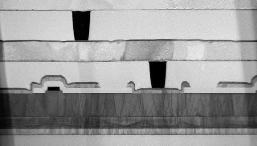
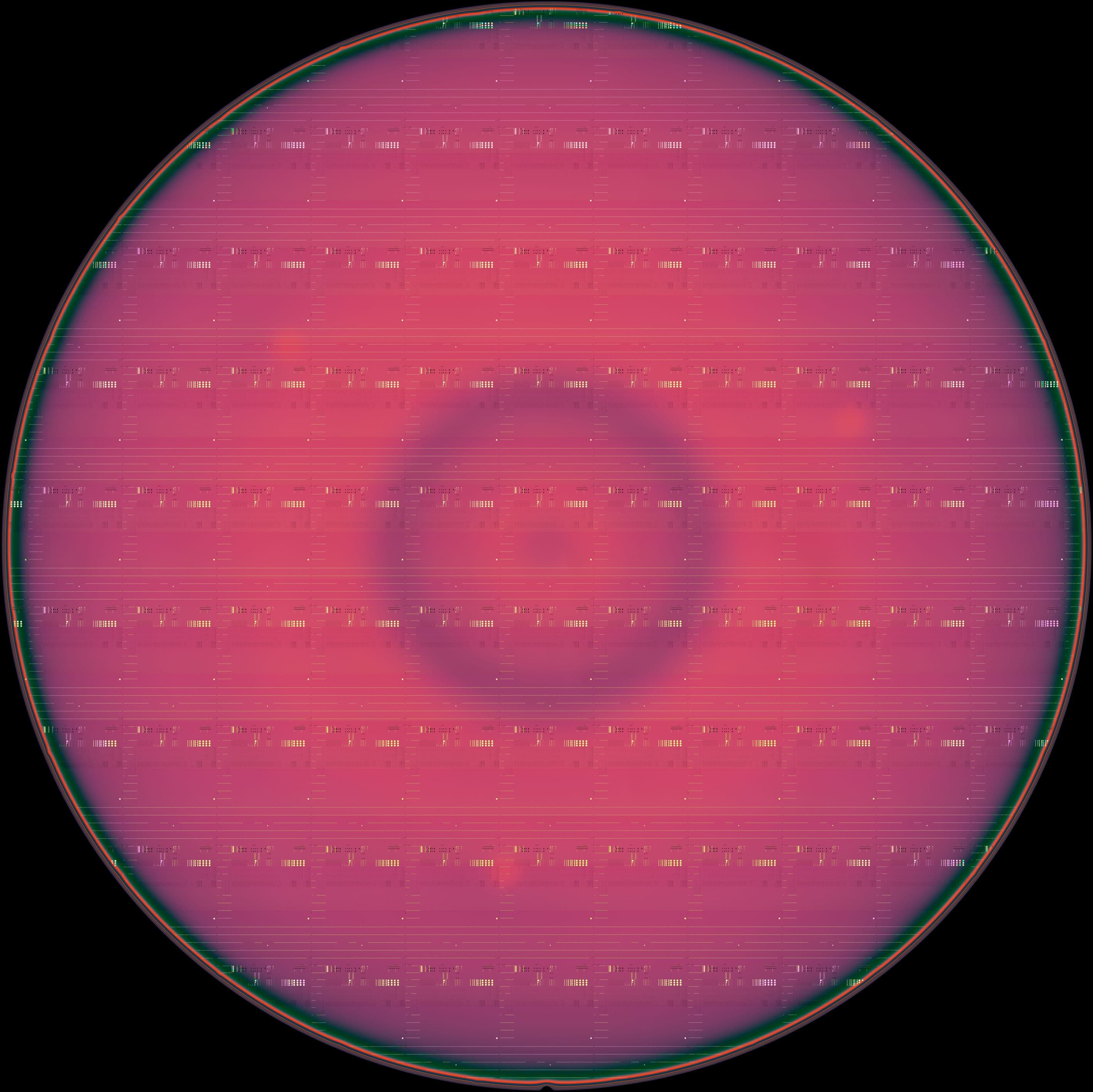
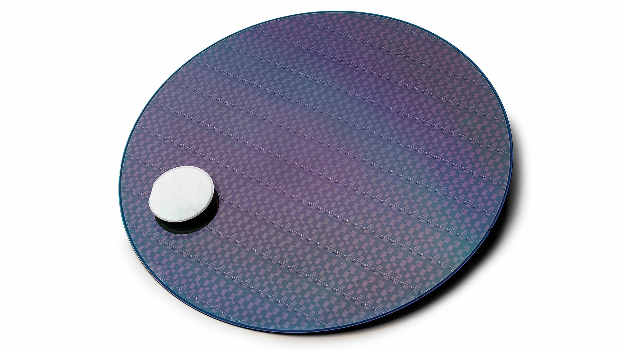
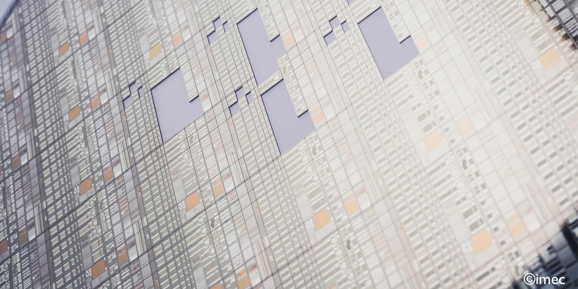
Imec researchers grew a GaN epi-stack epitaxially on a 200mm SOI wafer (Si(100)/SiO2/Si(111)) using metal-organic chemical vapor deposition (MOCVD). The stack consists of an AlN nucleation layer, an (Al)GaN buffer layer, a GaN channel layer, an AlGaN barrier layer and a Mg-doped p-GaN layer. Delicate strain engineering was performed to control the stress built up in the wafer during growth, resulting in a GaN-on-SOI wafer with a controlled warpage and good mechanical strength. In a next step, e-mode p-GaN HEMTs were processed and a TiN/p-GaN stack was used for the gate.
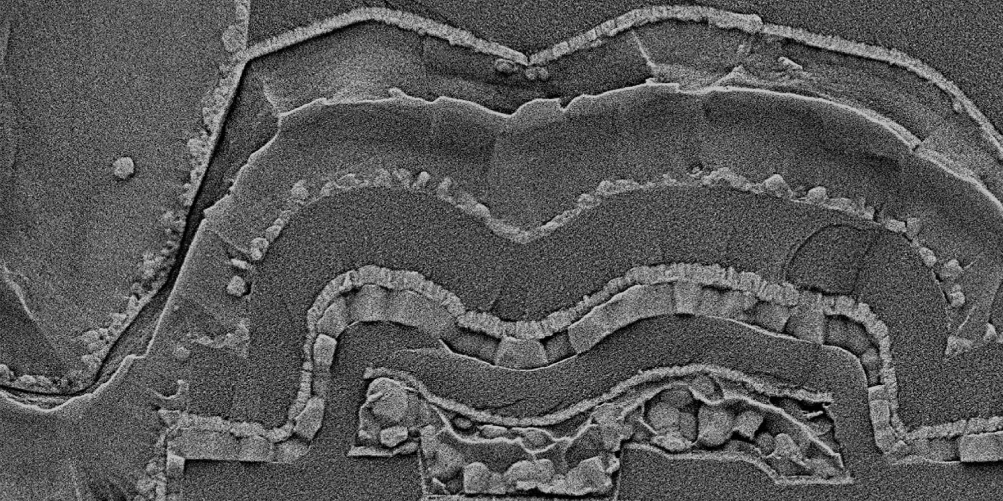
The HEMTs were then isolated horizontally as well as vertically by the combination of nitrogen implantation isolation and by trench etching through the (Al)GaN/Si(111) to the SiO2 buried layer. This way, a box-like isolation structure is created, surrounding each HEMT with an insulating dielectric.
Schematic cross-section of the e-mode p-GaN HEMTs.
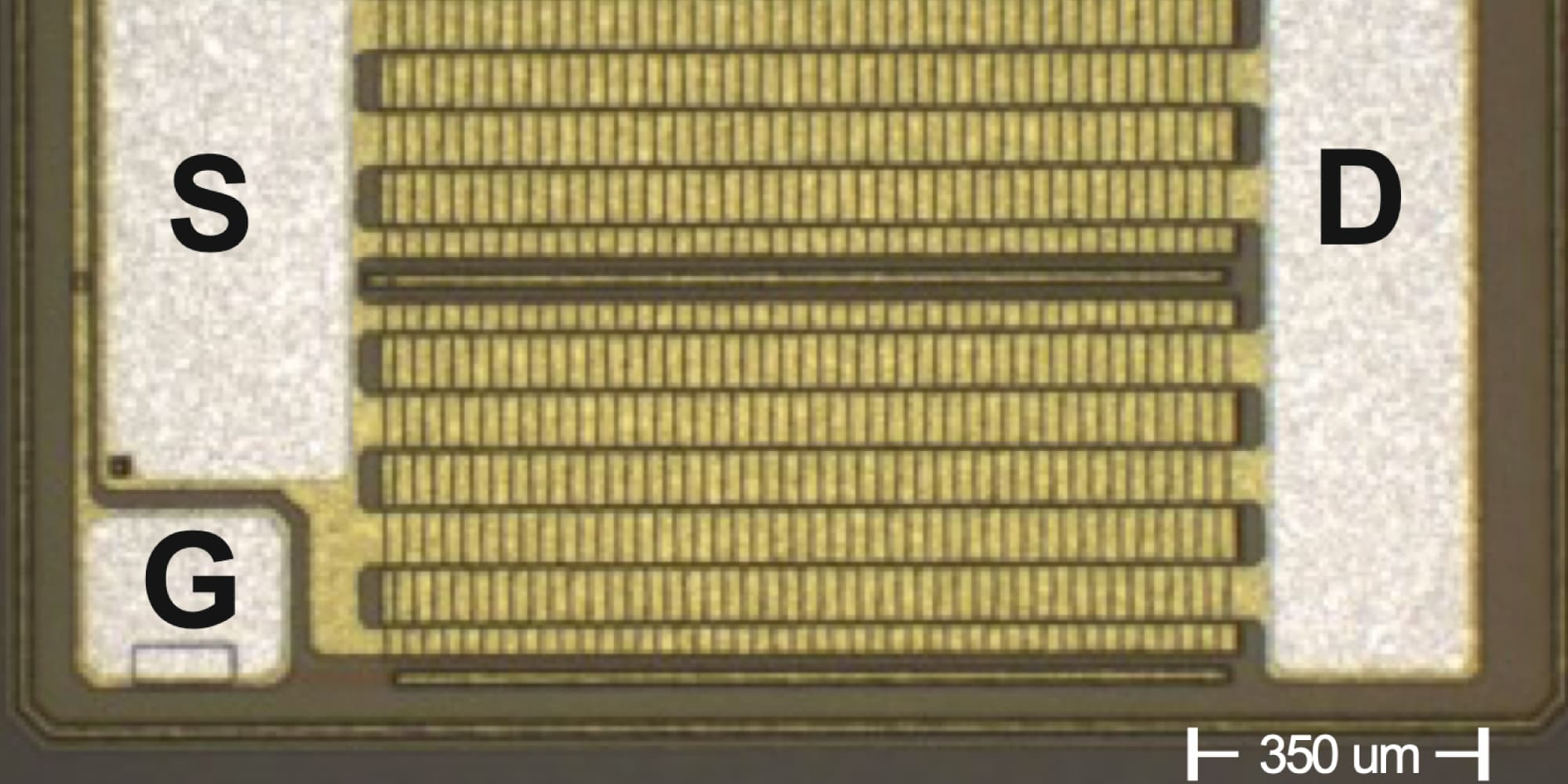
Top view of the fabricated device. A box-like isolation structure is created around each HEMT device.
The effectiveness of GaN-on-SOI device isolation
The p-GaN HEMTs on GaN-on-SOI have been fully qualified for 200V switching applications. Both the horizontal breakdown voltage of the trench isolation and the vertical breakdown of the SiO2 buried layer reach ~500V at 150°C.
(a) Horizontal breakdown of the trench isolation and (b) vertical breakdown of the SiO2 buried layer on the 200mm GaN-on-SOI at 25°C and 150°C.
The effectiveness of the device isolation becomes clear from the transfer characteristics of a HEMT device on GaN-on-SOI. These characteristics show the ID vs. VGS behavior of one device while the neighboring HEMT device is biased differently. The HEMTs are shown to be very robust when the substrate of the neighboring device is biased between -200V and 200V. This is in clear contrast to the performance degradation of devices on GaN-on-Si observed in similar experiments.
Transfer characteristics of a HEMT at 150°C (a) with common Si substrate biased from -200 to 200V (GaN-on-Si) and (b) while simultaneously biasing the neighboring Si(111) HEMT layer at different voltages (GaN-on-SOI).
With these results, imec researchers have demonstrated for the first time that using GaN-on-SOI in combination with trench isolation is a promising approach to monolithically integrate GaN power systems on the same wafer.
The research on GaN-on-SOI is part of imec’s Industrial Affiliation Program on GaN power devices. Within this program, imec takes today’s GaN-on-Si technology to a higher level of maturity and reliability, and explores new concepts for next-generation GaN technology. In this explorative track, imec focuses on new integration and device technologies, including novel substrates (such as GaN-on-SOI) and alternative isolation techniques (such as junction isolation and trench isolation).
The research is also carried out in the frame of the European ECSEL PowerBase project. PowerBase aims at developing the next-generation energy-saving chips based on materials such as GaN. Under the coordination of Infineon, the 39 project partners prepare these semiconductors for mass industrial use in smartphones, laptops, servers and many other applications. Within this project, imec looks beyond traditional substrate technologies for GaN-based devices, and explores novel isolation technologies. The PowerBase project receives funding from the Electronic Component Systems for European Leadership Joint Undertaking under grant agreement No 662133.
Want to know more?
- ‘200V enhancement-mode p-GaN HEMTs fabricated on 200 mm GaN-on-SOI with trench isolation for monolithic integration’, Xiangdong Li et al., IEEE Electron Device Letters
- Website on imec’s GaN Industrial Affiliation Program
- ‘Imec’s 200mm GaN-on-Si e-mode power devices withstand heavy ion and neutron irradiation’, imec press release
- ‘European ‘PowerBase’ to explore the next-generation power devices’, imec magazine
- Website on the PowerBase project
Published on:
5 June 2017

