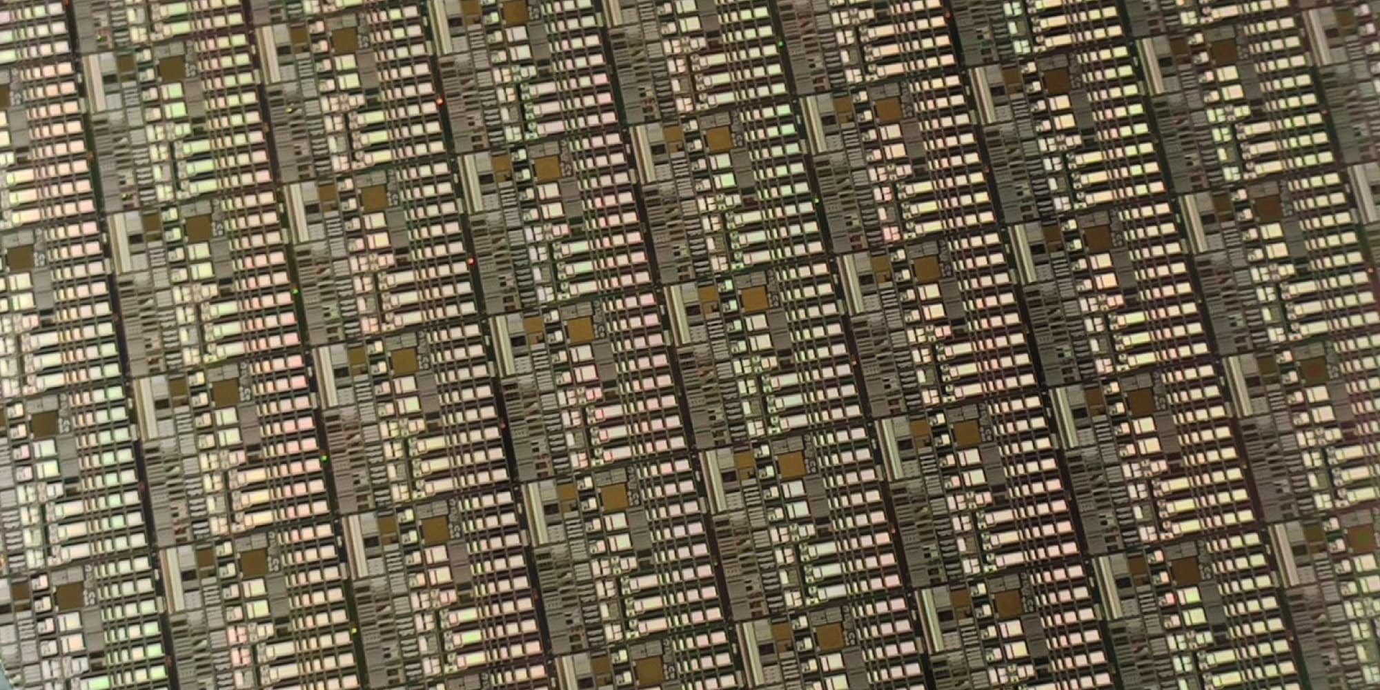
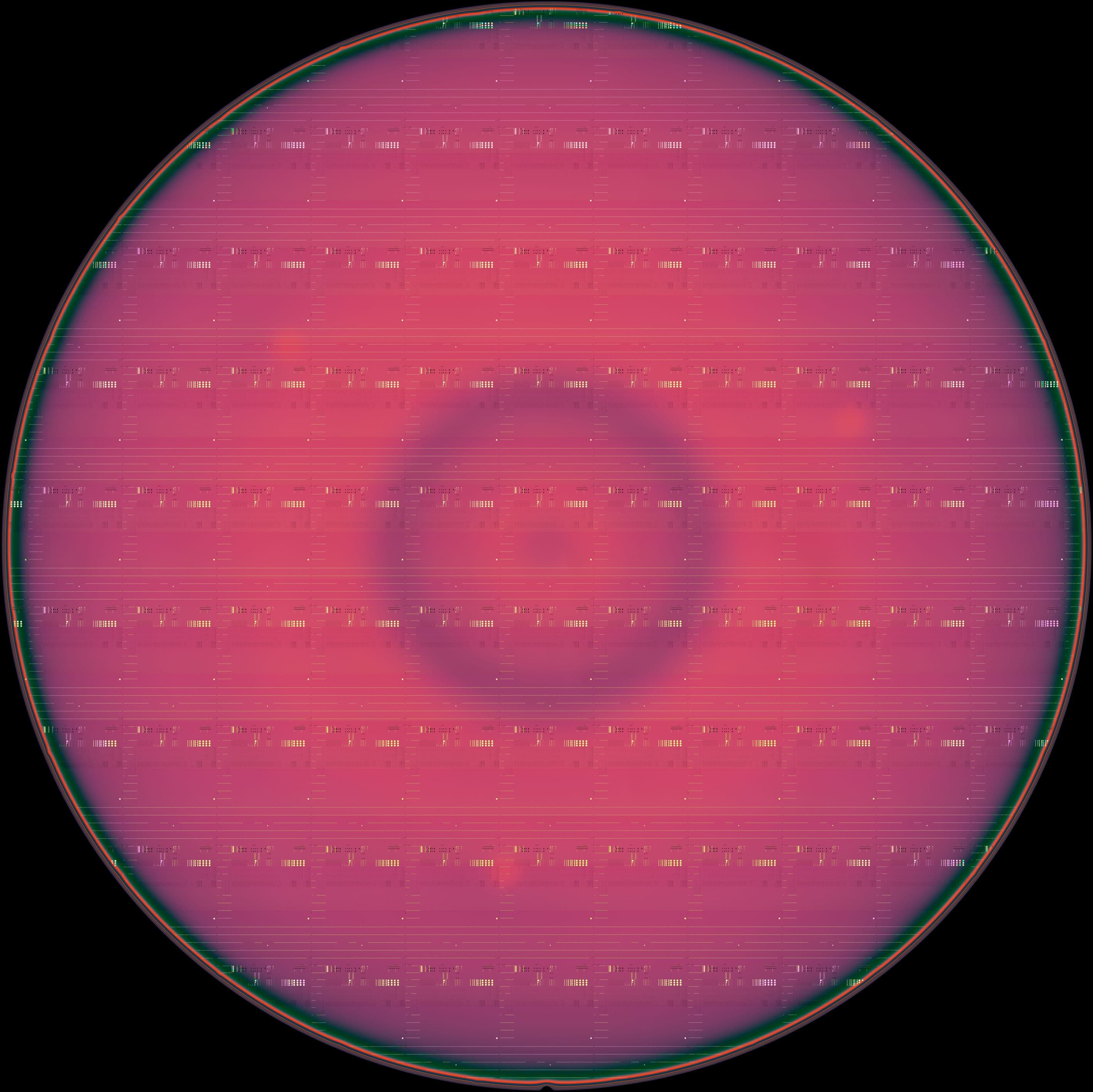
Gallium-nitride-on-silicon (GaN-on-Si) technology is maturing at a rapid pace and is being adopted in different markets. Target applications include high-voltage power switching and power conversion, RF power amplifying and sensing, battery chargers for mobile phones and for electric cars, and invertors for solar panel connections to the grid, to name a few. But GaN-on-Si technology has a considerable disadvantage: multiple GaN components (such as half bridges, high-electron mobility transistors (HEMTs) and drivers) have limited capability for being monolithically integrated on the same GaN-on-Si wafer. Therefore, today, GaN power electronics are dominated by off-the-shelf discrete components.
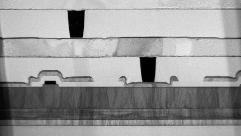
Imec researchers take a different approach: they combine GaN-on-SOI (silicon on insulator) with trench isolation to achieve monolithic integration. In an article that was recently published in Compound Semiconductor, Xiangdong Li, PhD student at imec, and Stefan Decoutere, program director GaN technology at imec, demonstrate the feasibility of this technology platform for developing the building blocks of an integrated all-GaN power IC.
Want to know more?
- Read the press release on the monolithic co-integration of a GaN half-bridge with drivers.
Published on:
15 May 2020

