The early days of system design
There was a time when the different steps needed to design and develop electronic systems were carried out in completely separated worlds. The engineers and scientists who populated the different worlds hardly talked to each other – there was no need for that – and each of them performed his own defined task in the best possible way.
Think about an electronic system that we’re all familiar with: the mobile phone. It is mainly composed of a screen, a battery and computer chips: a central processing unit (CPU, the ‘brain’ of the phone), a dynamic random access memory (DRAM) memory block (the ‘working memory’ of the brain), a data storage unit, communication chips, power distribution chips and many other small components.
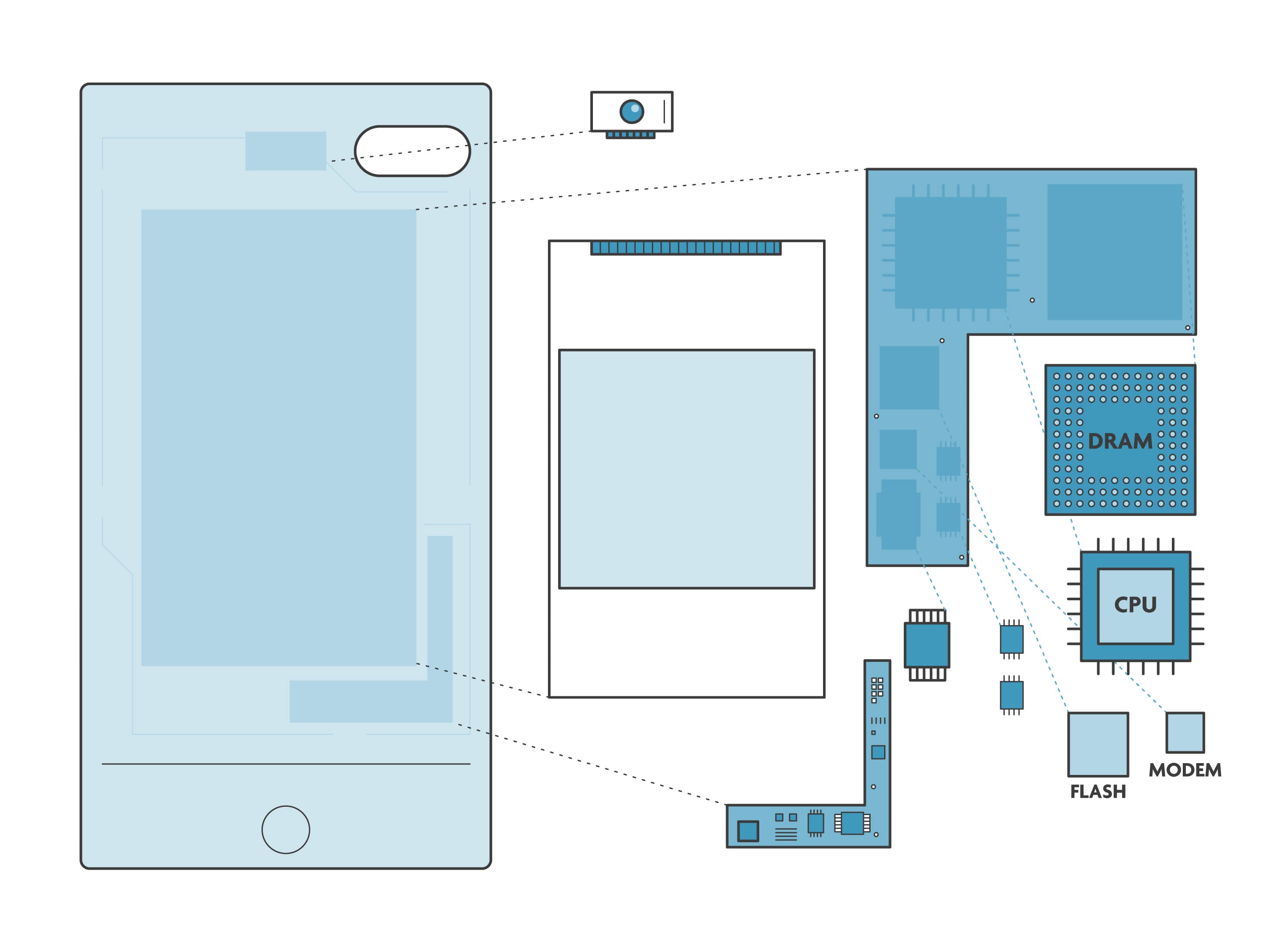
Figure 1: Main building blocks of a mobile phone – a schematic representation.
While mobile phone applications used to be simple (calling, texting, ...) they quickly became more complex (video, web, apps). To handle these new applications, mobile phone makers continuously had to optimize their phone for better performance, while keeping power consumption under control. To do this, they had to optimize the chips that are inside the phone. In the world of material scientists and device engineers, they would approach this challenge at the technology level. They chose for example the right material and the most optimal dimensions to make the transistors which are the smallest building blocks inside the different sub-systems that form the CPU, DRAM, communication chip etc.
Once the job of the technology engineers was done, they passed the characteristics of the transistor (such as current, voltage and physical dimensions) to the world of the designers. Without needing to know any further details of the chosen technology, they used this information to start building complex circuits. They made the right design choices so that each circuit efficiently would do what it needed to do.
When the requirements for power and performance were met, the circuit output was transferred to the engineers that put everything together. By puzzling the circuits together in a real chip, they created cost-effective solutions to pass on to the world of the software engineers.
There, the engineers looked for the appropriate algorithms to run real applications, so that the consumer could make a call or browse the web. They evaluated the power consumption and performance of the complete system when running these applications, making sure the software used the hardware efficiently.
For a long time, this independent way of working was the most efficient way to master the complexity of designing systems. In those days, chips already contained millions of transistors, organized into larger components and circuits. Fortunately, each piece of the puzzle (i.e., technology, circuit design, physical design, application) could be optimized independently, bringing the desired benefits for the end user.
Today’s mobile phones have become faster than a mid-80s supercomputer, faster than the laptop that many of us are carrying around. Phones became increasingly complex and powerful. More and more sub-systems have been added, extending the functionality of the phone with video, voice recognition, 4/5G and Bluetooth connectivity, gaming etc. Billions of transistors now reside inside these handheld devices. Through the years, the awareness grew that optimizing these systems needed a different approach. Our engineers started to realize that every choice they made to solve a problem – be it at the technology, circuit design, physical design or application level – induced a new problem that affected the whole system. For example, the technologists could make transistors operate faster, as before, but soon realized that this was at the expense of power consumption. It became more and more clear that gains could only be made if they would remove the boundaries between their worlds, start to collaborate and co-optimize the system across the different ‘worlds’.
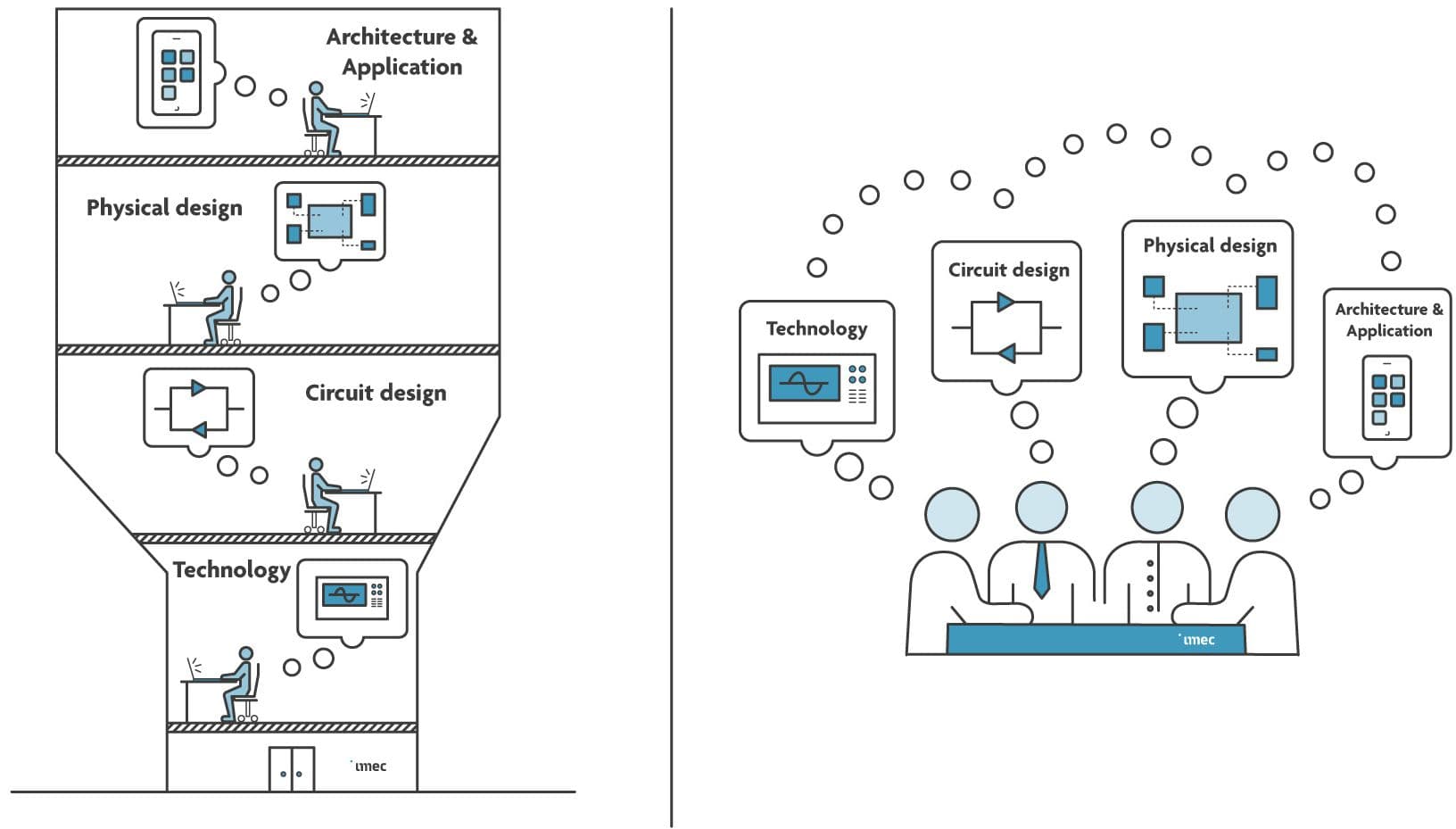
Figure 2: (Left) Schematic representation of the four different worlds of system design: (from bottom to top) technology, circuit design, physical design, and application. (Right) With increasing system complexity, the engineers representing these worlds started to collaborate and co-optimize the system across the different worlds.
In the semiconductor community, this evolution is referred to as design-technology co-optimization (DTCO), later complemented by system-technology co-optimization (STCO). Below, we will further clarify the need for these approaches and explain how they work. Throughout the article, it will also become clear how complex system design becomes when we leave the concept of separate worlds behind us. We therefore introduce a unique simulation framework. This helps designers manage the complexity of performing cross-‘world’ optimizations – in order to enable the grand applications of the future.
DTCO: history and examples
Until around 2005, the semiconductor community lived in an era of ‘happy scaling’ – driven by the Law of Gordon Moore. The continual shrinking of transistors yielded benefits for the whole system in terms of power consumption, performance, area and fabrication cost (denoted as PPAC). To put it simply, performance was increased because the length of the transistor’s gate was decreased (the gate being an essential part of the transistor that controls the flow of electrical current that runs through the transistor’s conduction channel); power consumption lowered because the supply voltage could be down-scaled; area decreased because of the smaller dimensions; and fabrication costs were reduced because more transistors could be processed on one single wafer. Roughly every two years, the semiconductor industry was able to introduce a new, more powerful technology generation – denoted as the ‘x’nm technology generation (or node) – with the double amount of transistors populating the same chip area.
The first signs of trouble came about 15 years ago, right after the introduction of a completely new gate structure (known as high-k/metal gate) in the 45nm technology generation. This new gate stack was introduced to overcome current-leakage issues that popped up with further transistor scaling. But it also changed the properties of the transistor, whose performance behavior (in terms of current and voltage) started to deviate. With further scaling, changes in the design were needed to compensate for this behavior – marking the end of the happy scaling era. Technologists and design engineers began to see the benefits of optimizing technology and design together [1]. The first steps towards design-technology co-optimization (DTCO) had been taken. From the 2xnm nodes onwards, DTCO became a commodity.
For the development of the 1xnm technology nodes, structural scaling boosters were introduced as an additional enabler for the DTCO work. These boosters allow to further reduce the area – not at transistor level but at cell level. Cells can be considered the smallest functional circuits that can be created from the transistors. Think about a memory cell, able to store one bit of information. An example of a structural scaling booster is a self-aligned gate contact, which allows to place the contact to the transistor’s gate directly on top of the transistor, enabling a reduction of the overall contact area. With these scaling boosters, cells could be further scaled to an extreme level of compactness.
Throughout the years, DTCO also became an interesting tool for assessing the benefits (at cell level) of introducing completely new technologies in chip manufacturing processes. To continue the path of transistor scaling, technologists are indeed exploring new ways of building transistors for logic as well as for memory applications. A well-known example is the introduction of the FinFET transistor in the 14nm technology node, yielding better performance than ‘good-old’ MOSFET for scaled dimensions. Also for memory, research institutes such as imec explore a myriad of novel technologies – to replace some of the traditional memory technologies or to allow for optimized memory usage in traditional computer architectures.
At imec, for example, we used DTCO to assess the power-performance-area benefits of introducing a more disruptive technology in the computer’s cache memory.
Cache memory is a very small type of memory that resides close to the processor to enable fast access to data. This type of memory is typically organized as a hierarchy of different cache levels. The role of the cache memory is usually filled by the high-speed static random access memory (SRAM). Throughout the years, the SRAM bit cells – typically made up of 6 transistors – have been downscaled to increase the memory density and hence the capacity of the cache. But below the 10nm technology node, SRAM scaling has become very challenging, due to the increased power dissipation when memories are not active (leakage) and reliability issues. Memories like the spin-transfer-torque magnetic random access memory (STT-MRAM) are promising alternatives for SRAM as last-level caches. It is non-volatile in nature, which means that it retains data even when the system is shut down. This effectively solves the problem of SRAM memories ‘leaking’ energy when they are inactive. STT-MRAM memory cells are also much smaller than SRAM cells. However, it is challenging to write into them efficiently at high speeds. With DTCO, our teams were able to define the requirements, specifications and trade-offs for STT-MRAM memories – for example: we show that for a single cache access, writing to STT-MRAM can be more energy efficient than SRAM at larger cache sizes [2].
Figure 3: At larger cache sizes, writing to STT-MRAM is more energy efficient than writing into SRAM: a DTCO result.
STCO and why we need it
Today, the semiconductor industry has 5nm chips in production, with FinFETs being the transistor of choice. Some of the chip makers are preparing to move to the 3nm and 2nm technology generations by implementing gate-all-around nanosheet transistor architectures. At the same time, research institutes such as imec explore the options for sub-3nm technology nodes. For these scaled nodes, however, the benefits of what DTCO can bring are saturating. With only a few scaling boosters left in the toolbox, further scaling the cell area without jeopardizing power and performance has become extremely challenging.
So why not expand the idea of co-optimizing design and technology towards the other ‘worlds’ – referred to as ‘higher abstraction levels’ – including bigger circuits and eventually the system application domain? What if we could introduce new technologies and evaluate their impact at the system level, when running real applications? Can we not at the same time re-think the way we place and interconnect the various sub-systems or re-consider the power delivery network in order to obtain additional gains for the whole system? This approach is called system-technology co-optimization (STCO).
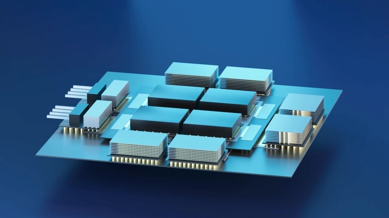
An STCO-oriented approach may involve the dis-integration and re-partitioning of the original system. Think about a microprocessor and its cache memories. Traditionally, these memories are placed close to the microprocessor, always in the same plane. But we could as well move some of the cache memories to a different chip and place this chip on top of the processor – using so-called 3D integration techniques such as wafer-to-wafer bonding. As the cache is now closer to the processor, data travels a much shorter distance, potentially improving latency and speed.
In industry, we see more and more examples of systems being built based on a smart functional (re-)partitioning of the system. The approach is interesting, as it allows to optimize the different sub-systems separately. In the happy scaling era, all the different sub-systems (such as logic or memory) were hooked onto one and the same technology platform. For example, 14nm FinFETs were used to build the logic processor, the SRAM cell as well as the analog blocks of the system. But with STCO, different process technologies – even multi-node variations of one technology – can be used to better answer the different needs of the various sub-systems. For example, when moving the memory sub-system to another chip, it does no longer need to be process-compatible with the logic sub-system: it can be optimized and processed on a separate wafer. This gives more flexibility in building new systems – systems that can for example run artificial intelligence applications – answering the need for more diversification.
With this evolution, the number of possible ways to build a system is increasing dramatically, and choices need to be made very carefully. In addition, a growing number of new technologies is being explored as alternatives for the older, more traditional technologies. In other words, there is a plethora of choices to be made in designing future systems.
The expanding scope of the memory landscape is a good example. While STT-MRAM might replace SRAM in last-level caches, more disruptive alternatives are being explored for the DRAM memory as well – as to further increase DRAM memory density. Besides, industry looks at a range of emerging memories that can help fill the gap between the computer’s fast main memories (DRAM and SRAM) and the slower but higher-density storage solutions (SSD cards where huge amounts of data are stored in a NAND Flash-type of memory cells). These ‘in-between’ memories, called storage class memories, can potentially address some of the main bottlenecks in standard computing architectures.
The SEAT platform
The more abstraction layers we can include in our co-exploration, the more profit this will bring to the system level. But our team also realized that this goes hand in hand with a dramatic increase in complexity. Mastering such a comprehensive optimization process is extremely challenging. The process of co-optimizing all those many knobs at many different abstraction layers is not a task that is manually feasible. Therefore, we developed a unique framework that enables easy, fast and detailed design space exploration, throughout the various abstraction layers. This platform is called SEAT – short for System benchmarking for the Enablement of Advanced Technologies. It can help companies design their system using optimal technology for the different parts of the system.
SEAT essentially consists of different simulation tools that are integrated together in a specific workflow, enabling us to perform cross-layer optimization. Some of the simulation tools are developed in-house, others are extended based on open-source community efforts (such as gem5, which is at the heart of our application simulation tool).
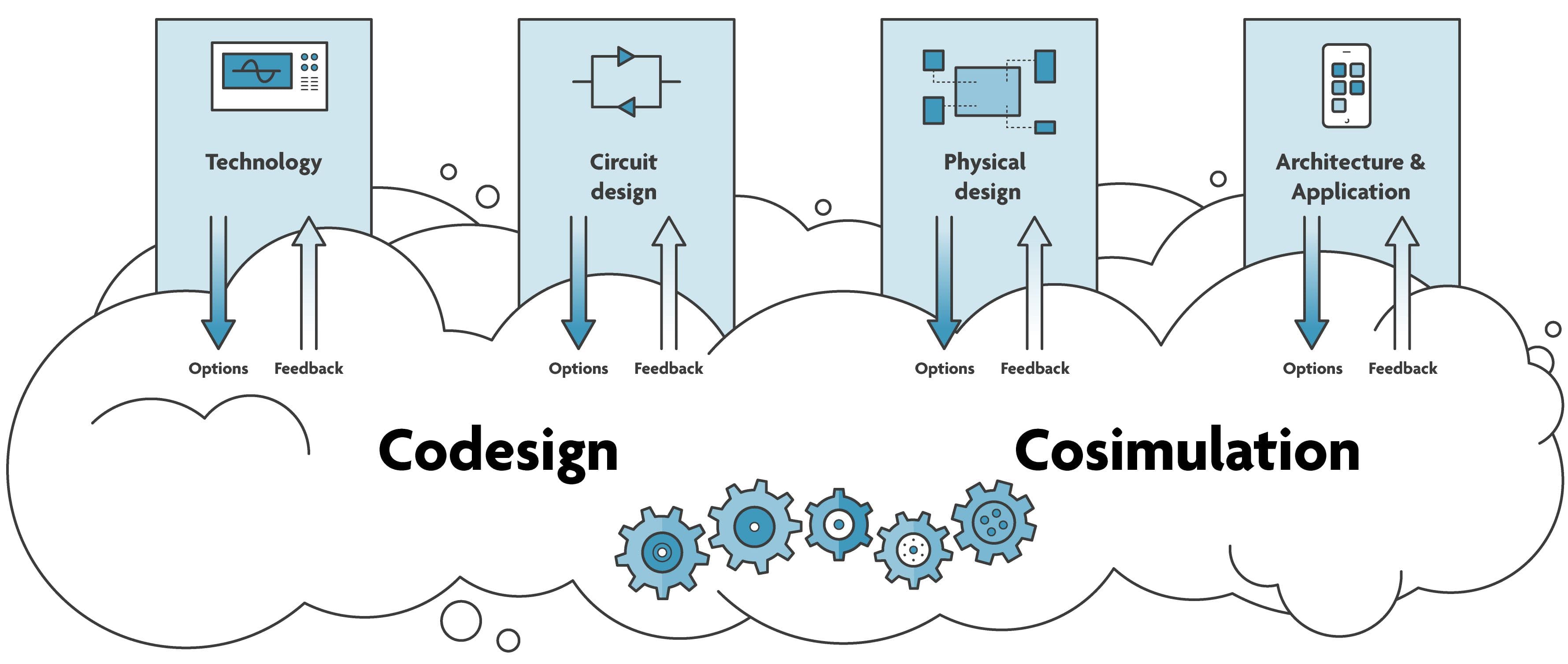
Figure 4: Simplified representation of the SEAT flow.
The SEAT workflow starts with each abstraction layer offering multiple options with different trade-offs. Each of the abstraction layers feeds these options in the simulation framework using a standard interface, where different design tools interact to simulate all these different options across the stack. The simulation framework outputs the power-performance-area-cost (PPAC) benefits at the system level for any application running on a range of architectures, designed with new components, using emerging technologies. This results in important feedback, because it allows to accurately evaluate optimizations, considering effects at all layers.
As an illustration of what SEAT can do, let’s go back to the previous example where our team explored the feasibility of replacing SRAM with STT-MRAM for last-level cache memory applications. Our DTCO work helped us finding the technology specifications for the STT-MRAM bit cell. Going one step further, we have extended this work towards the system level. The effect of a cache technology on the system’s energy and performance indeed not only depends on the technology, but also on the cache circuit design, on the overall system architecture and on the applications being executed. With the help of SEAT, we obtained an optimized design for the cache circuit, leading to additional gains at the system level. More particularly, improved performance and power consumption could be demonstrated by optimizing the number of banks in the cache design – a bank being a sub-structure of the cache [3].
Figure 5: By using SEAT, STT-MRAM-based cache circuit design could be further optimized.
Future plans
Our team will continuously extend the simulation framework with a broader range of technologies – all developed in-house. These include advanced technologies for logic applications, advanced wiring schemes, emerging memory technologies, 3D integration technologies and many more.
In parallel, we aim to explore increasingly larger and more complex heterogeneous systems. So far, we used our framework to optimize systems-on-chip (i.e., circuits that integrate most components of an electronic system on one and the same chip), or to combine a limited number of chips (such as memory and logic chips) into one system. We will gradually expand our scope towards bigger systems, made up of a broader variety of chips. Think about optical input/output (I/O) chips – chips for e.g. data center applications that allow to convert electrical signals into optical signals and vice versa and transmit these signals via optical fibers. Or think about analog sensing chips, or chips for machine learning applications. In the longer term, we plan to investigate the feasibility of evaluating technologies and systems at full data center scale. Obviously, the rise of complexity will come with many challenges.
Our cross-layer methodology will help companies design the most optimal system using the right technology for the different parts of the system. The SEAT platform has been developed within the IIAP (imec international affiliation program) framework of imec, i.e. within the Memory and Memory INSITE IIAPs. The IIAP creates a research ecosystem for accelerating the development of intellectual property, sharing R&D resources and risks, providing companies a cost-effective way to extend their research and product development capabilities.
This article was originally published in Semiconductor Digest, June/July 2021, pgs 18-22.
Want to know more?
[1] L. Liebmann et al.,"Demonstrating the benefits of template-based design-technology co-optimization," Proc. SPIE 7641, Design for Manufacturability through Design-Process Integration IV, 76410R (2 April 2010); https://doi.org/10.1117/12.848244
[2] S. Sakhare et al., "Enablement of STT-MRAM as last level cache for the high performance computing domain at the 5nm node," 2018 IEEE International Electron Devices Meeting (IEDM), San Francisco, CA, 2018, pp. 18.3.1-18.3.4, doi: 10.1109/IEDM.2018.8614637.
[3] T. Evenblij et al., "A Comparative Analysis on the Impact of Bank Contention in STT-MRAM and SRAM Based LLCs," 2019 IEEE 37th International Conference on Computer Design (ICCD), Abu Dhabi, United Arab Emirates, 2019, pp. 255-263, doi: 10.1109/ICCD46524.2019.00039.
Timon Evenblij joined imec in 2017 after receiving his M.S. degree in computer science engineering from Ghent university, summa cum laude. As system memory architect, he is working on evaluating and optimizing the use of emerging memory technologies in complex systems running real applications, by means of architectural simulation and performance analysis tools. He is interested in system level design, bridging the gap between hardware and software.
Manu Perumkunnil Komalan (M) completed his Integrated Masters in Nanotechnology from Amity University, India in 2011. He received his Ph.D. in Electrical Engineering from Katholieke Univ. Leuven, Belgium and in Computer Science from Universidad Complutense de Madrid in 2017. He then joined imec as a memory system architecture researcher. His research activity primarily involves exploration, analysis and optimization of NVMs across the different layers of abstraction. Currently, he is the Project Lead for the Memory INSITE program at imec.

Gouri Sankar Kar received his Ph.D. in semiconductor device physics from the Indian Institute of Technology, Kharagpur, India, in 2002. From 2002 to 2005, he was a visiting scientist at the Max Planck Institute for Solid State Research, Stuttgart, Germany. In 2006, he joined Infineon/Qimonda in Dresden, Germany, as lead integration engineer and was responsible for vertical transistor development for the DRAM application. In 2009, he joined imec, Leuven, Belgium, where he is currently working as the VP R&D Compute & Memory Device Technologies

After completing his PhD in imec, Arnaud Furnémont joined Intel in Boise and became responsible for 20nm planar Flash reliability, and later on X-Point. In 2013 he came back to imec and served as memory device manager, then memory director with MRAM, SCM, 3D NAND and ferroelectric memory as main focuses. Since 2019, Arnaud expanded his responsibilities to become compute and memory VP for device and integration.
Published on:
31 August 2021


