Investigating the Impact of Process Parameters and Substrate Properties on Wafer Bow after Temporary Bonding
Master projects/internships - Leuven | Just now
Explore how process conditions and substrate properties influence wafer bow in advanced semiconductor manufacturing and gain hands-on experience optimizing bonding processes through design of experiments.
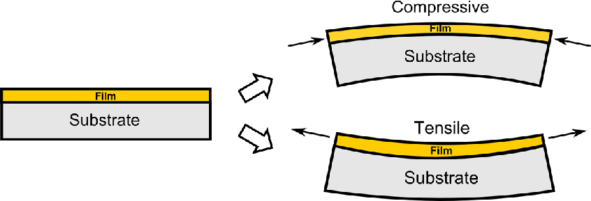
Temporary bonding is a crucial technology for enabling 3D integration, particularly as advancements push wafer thinning to extreme values like 3-5 µm post-bond wafer bow becomes a critical factor since excessive bow can lead to device cracking due to stress and handling failures in downstream processes.
In this internship, we will apply Design of Experiments (DOE) to identify the key process parameters influencing post-bond bow. Following this initial phase, the bonding process will be optimized to achieve minimal bow.
Given the significant role of thermal conductivity and coefficient of thermal expansion, the developed model will be further tested on different substrate types to assess its broader applicability.
Type of Project: Combination of internship and thesis
Master's degree: Master of Engineering Technology; Master of Engineering Science; Master of Science
Master program: Chemistry/Chemical Engineering; Electromechanical engineering; Mechanical Engineering; Materials Engineering; Physics
Duration: 3 - 6 months
Supervisor: Kristof Paredis
Supervising scientist: Jakob Visker
For more information or application, please contact Jakob Visker (jakob.visker@imec.be) and Kristof Paredis (kristof.paredis@imec.be).
Imec allowance will be provided.