Silicon photonics foundry services
Do you need access to silicon photonics prototyping and manufacturing services? Leverage imec’s 200mm and 300mm Si and SiN photonics platforms, featuring a wide variety of passive and active components.
This enables you to directly connect with imec’s cutting-edge expertise and infrastructure in this domain, creating advanced photonic integrated circuits (PICs) in scalable volumes, all the way to commercialization, in imec’s cleanrooms or at partnered foundries.
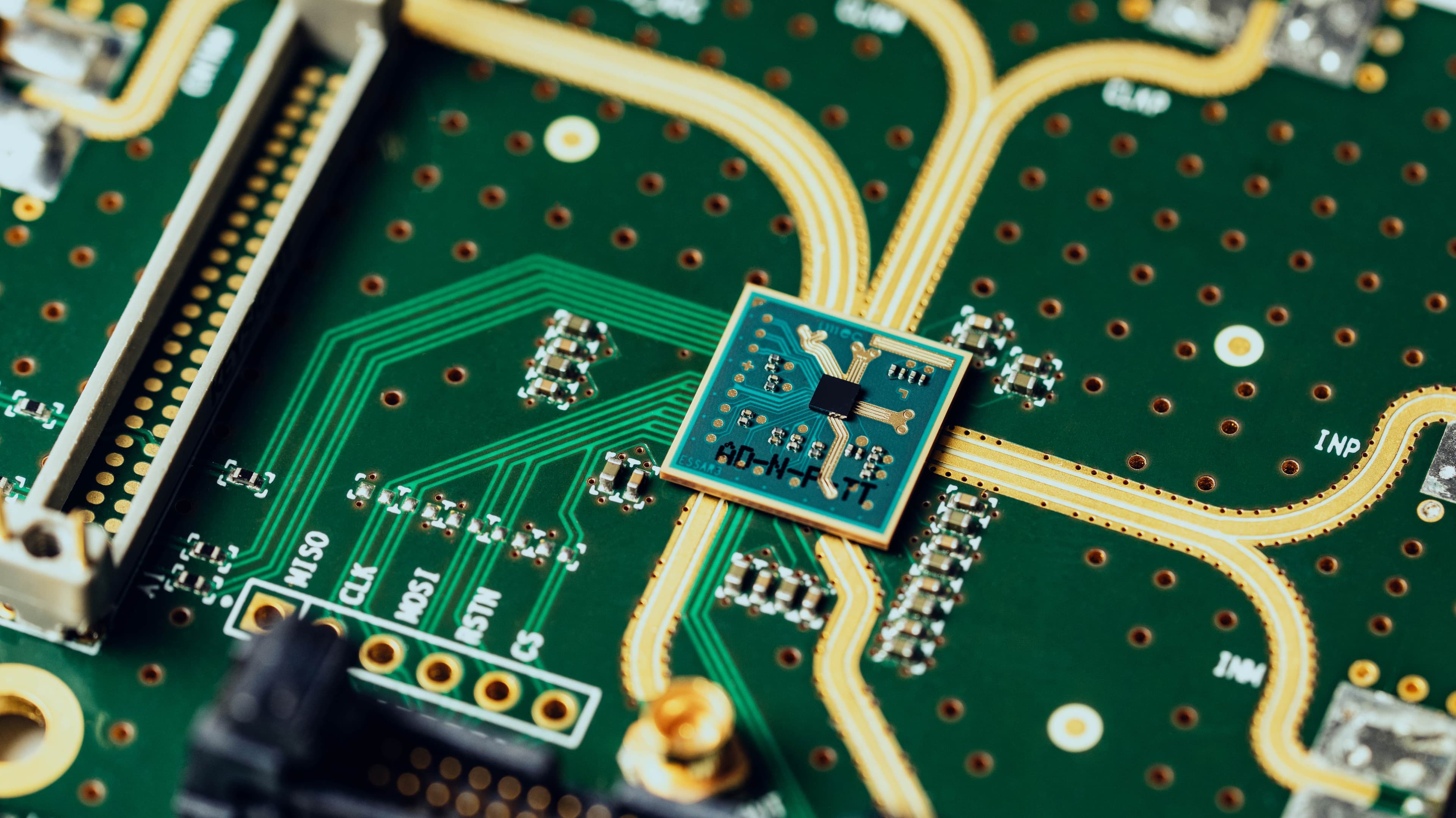
200mm silicon photonics platform: iSiPP200
Imec’s iSiPP200 is a mature 200mm silicon photonics platform with a comprehensive silicon-validated PDK. It’s possible to integrate high-quality silicon nitride (SiN) waveguides, and to add III-V lasers through flip-chip bonding at wafer scale.
In addition, integration of LNO modulators, III-V lasers and SOAs is available through micro-transfer printing.

You can access this platform via both dedicated (full-mask) runs or, for a subset of technologies, via multi-project wafers (MPW) through IC-Link.
Click here for more info on iSiPP200 prototyping and manufacturing services
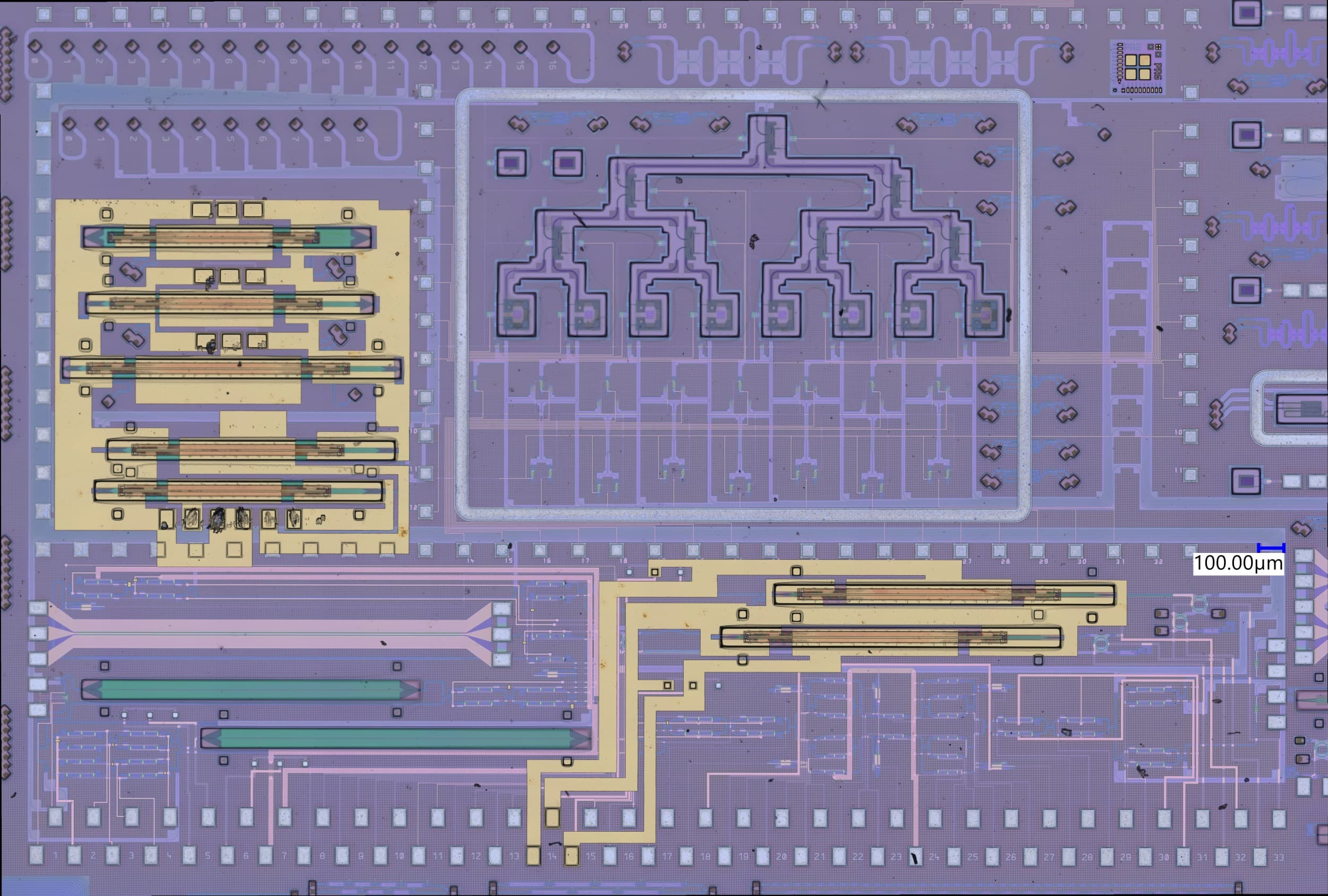
300mm silicon photonics platform: iSiPP300
For next-generation silicon photonics, you can access imec’s 300mm photonics platform. In addition to all standard building blocks, this platform includes exploratory options such as through-silicon vias (TSV), microbumps, and embedded microbumps.
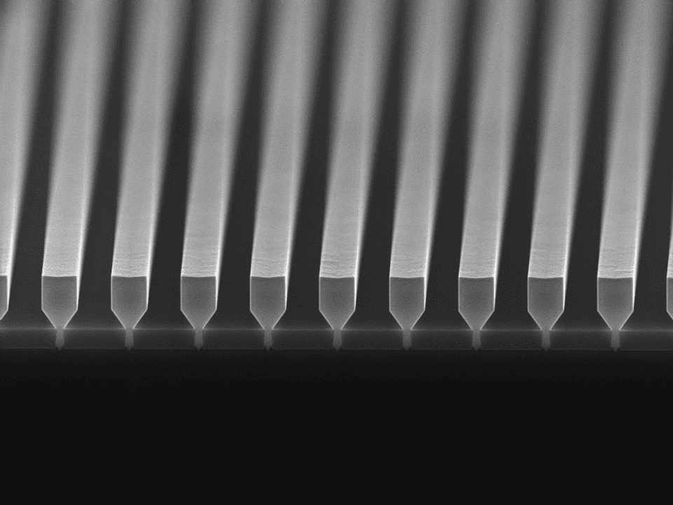
200mm and 300mm silicon nitride photonics platforms
Depending on your application, different silicon nitride photonics technologies are available to you:
- LPCVD waveguides (200mm) for applications requiring ultra-low loss, such as photonic quantum applications and data/telecommunication.
- PECVD waveguides (300mm) for applications such as integrated photonics on CMOS imagers and flat optics.
- Integration of active components such as lasers, modulators and photodetectors (200mm).
Integration of SiN photonics in complex build-ups with technologies such as CMOS and non-standard SOI photonics is also possible.
Facilitating expertise
To tailor imec’s silicon photonics platforms to your application, we offer supporting services to our customers, such as:
- Design and IP services, to be considered upon request
- Management of your PIC supply chain
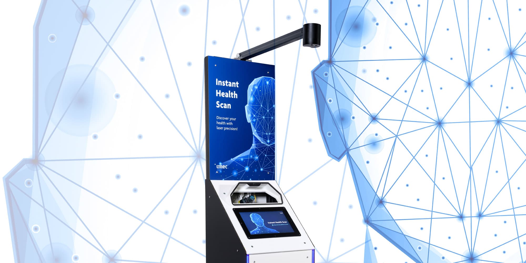
Work with us
Are you looking to accelerate your development?
Imec not only helps you to address technological challenges. Thanks to our thorough knowledge of the integrated photonics ecosystem, we can function as your full-fledged strategic partner – right down to venturing support.
Click the button below to get in touch.