No technology platform can do it all in integrated photonics. In this article, we take a closer look at a base material that stands out for its seamless integration with existing CMOS infrastructure: silicon.
Capable of propagating high data rates at relatively low power dissipation, light is a fantastic carrier of information. Silicon has been the cornerstone of semiconductor technology for decades. It was only a matter of time before two and two were put together: a technology that harnesses the power of light using the very same platform that propelled microelectronics to great heights. After all, why reinvent the wheel when billions and billions of dollars had already been sunk into perfecting the materials and processes used to manufacture microelectronics?
And so silicon photonics was born. First explored in the 1980s and starting to gain steam around the turn of the century onward, by now the technology has been commercialized in volume. It’s proving increasingly popular in data centers, in which silicon photonics-based transceivers enable optical connections between servers.
As the world’s hunger for data grows, as well as its desire to reduce energy consumption, the technology is expected to balloon in the next decade. Yole Group, a market researcher, projects a blistering compound annual growth rate (CAGR) of 36 percent for the silicon photonics market over 2021-2027, reaching almost 1 billion dollars by the end of that period.
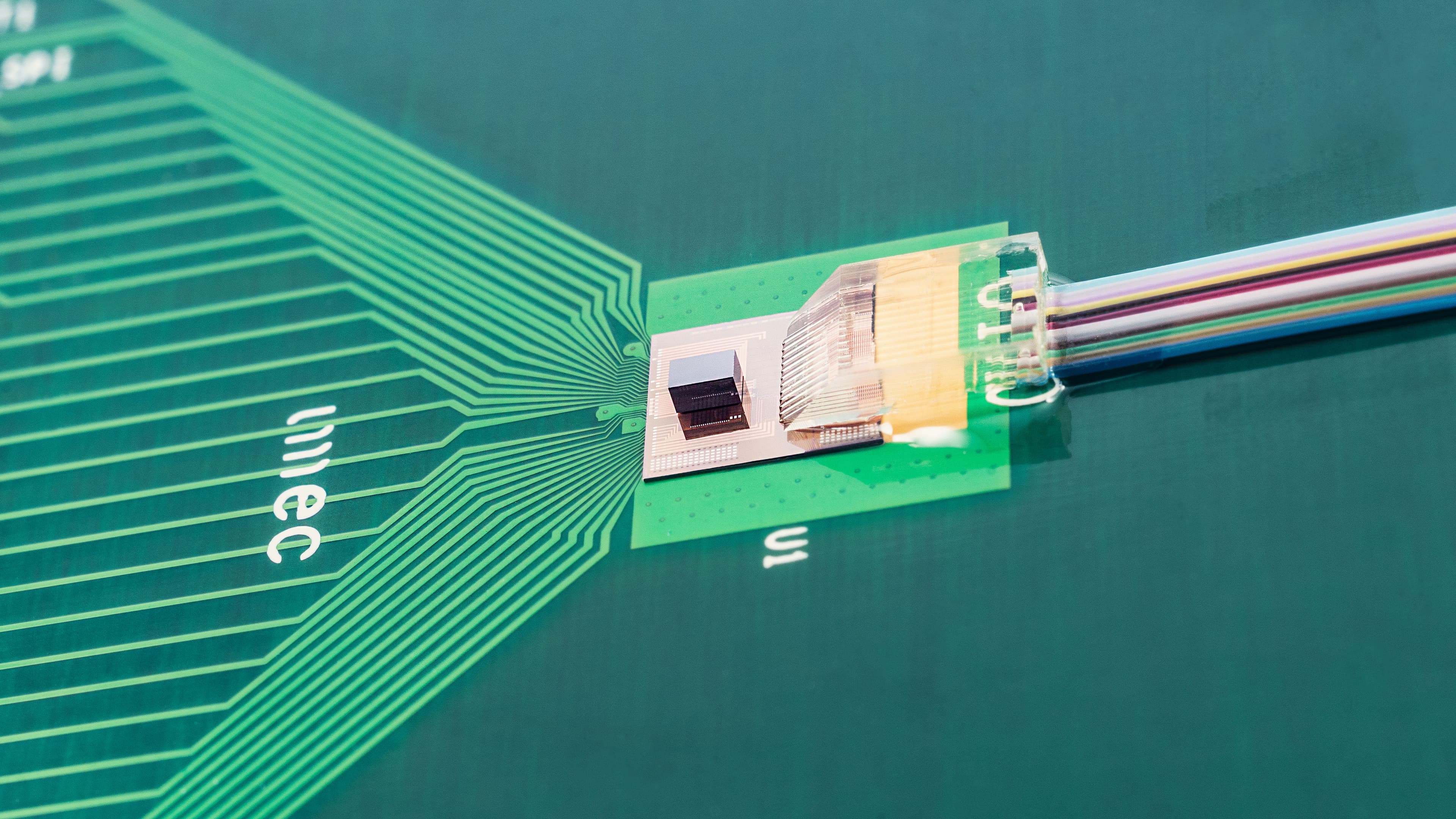
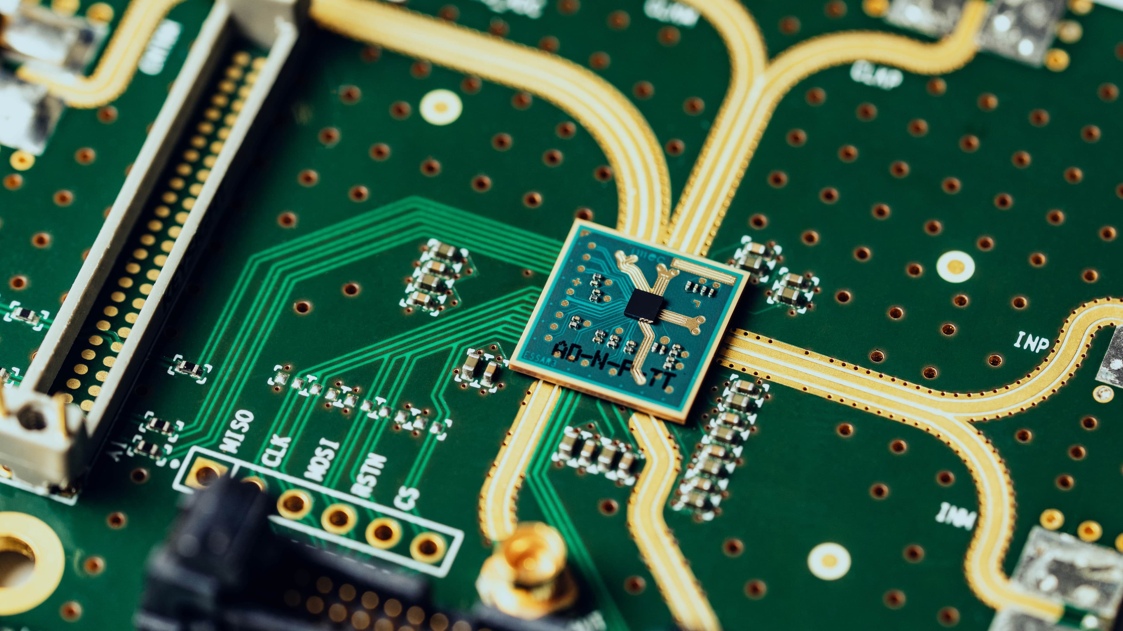
A hybrid CMOS-silicon photonics transceiver prototype developed at Imec. Credit: Imec
While the main driver of that growth is intra-data-center communication, emerging applications are expected to pile on. Silicon will likely be used for data exchange over increasingly shorter distances, and ultimately between chips in the same system. The technology is also in the running as a base platform for automotive lidar, allowing autonomous vehicles to navigate roads, or at least helping drivers to avoid collisions.
“Silicon photonics is produced in 300mm standard semiconductor foundries. That means it can be produced with tight specs and quality control and reliable logistics. This offsets some of its limitations and makes it an attractive baseline in combination with other technologies, such as lasers,” explains Carol de Vries, chief technology officer at Photondelta. Preliminary market prognoses suggest that silicon photonics, alone or in combination with other integrated-photonics platforms, is here to stay, he adds. “It’s expected to sport a market share of 45 percent by 2040.”
Plenty of scope
Traditionally, silicon photonics (SiPh) is understood to mean integrated photonics based on the materials that dominate regular electronic circuits: silicon and silicon oxide (silica). In scientific literature, this type of integrated photonics is commonly referred to as silicon-on-insulator (SOI), a term also in use for specialty semiconductor technology.
In this strict sense, SOI may be the most limited technology in the three-membered integrated-photonics family, which also includes silicon nitride (SiN) and indium phosphide (InP) based technology. Owing to its indirect bandgap, silicon is unable to produce gain or lasing, ie the material can’t be used to build active components such as light sources and amplifiers. That’s also the case for SiN, but this material features lower light losses and broader spectral coverage than SOI.
InP is the only semiconductor that can perform all functions without outside help but shares SOI’s downsides with respect to losses and spectral coverage. Both the Si and the SiN platform typically depend on some form of integration with InP, if only as a light source. The best way to do that is application-specific.
Of course, SOI’s properties are good enough for many interesting applications. Light can be efficiently led in and out of the chip, and important passive components such as gigahertz-capable modulators and photodetectors are available. Add to this the ability to piggyback on decades of experience in silicon processing – 300mm wafers, high yield, co-integration with CMOS, a variety of advanced and 3D-integration techniques – and there’s plenty of scope for silicon photonics.
Forbidden
Increasingly, however, SiPh is interpreted as any type of integrated photonics that can be manufactured in a CMOS fab. In that case, SiPh and SiN morph into a single entity, since the latter is CMOS-compatible as well. But there’s a caveat, Imec Fellow Silicon Photonics Joris Van Campenhout explains. “Manufacturing high-end SiN waveguides, with very low light losses, requires high thermal budgets. That may not be compatible with co-integrating other functions.”
Maintaining CMOS compatibility comes with constraints in general. Van Campenhout: “A CMOS manufacturing environment is strictly controlled. Certain materials are forbidden, including InP and other III-V semiconductors.” On the other hand, CMOS’ commandments aren’t written in stone; over the past decades, several new materials have been introduced in the fab to keep Moore’s law going. “If you have a strong business case, anything is possible. Currently, however, there aren’t any integrated-photonics applications that generate the kind of volumes that would warrant such adaptations in mainstream fabs.”
Van Campenhout notes, however, that future use cases require SiPh to introduce new materials, to keep making improvements in performance and cost. For example, as the signal rate in data center transceivers grows beyond 200 Gb/s, realizing enough modulator bandwidth with acceptable light losses becomes challenging. Such roadblocks can only be removed by introducing new materials into the mix. “Enriching SiPh with new materials and new functionality while maintaining maximum CMOS compatibility represents a great opportunity.”
It’s possible to introduce new materials while adhering to CMOS rules by integrating ‘forbidden’ materials or components containing these materials outside the front-end processing environment, ie at the back-end-of-line. “Today, it’s unclear what’s the most appropriate level of integration, and when that’s going to happen at scale. Apart from data and telecom, application research is still in its infancy. Which functions do you need to integrate? What specifications are required? These are questions we still can’t answer for a wide range of applications. Still, I think it’s fair to say that as SiPh gains traction, business models solidify and market pull increases, boundaries will prove not as hard as they were once thought to be.”
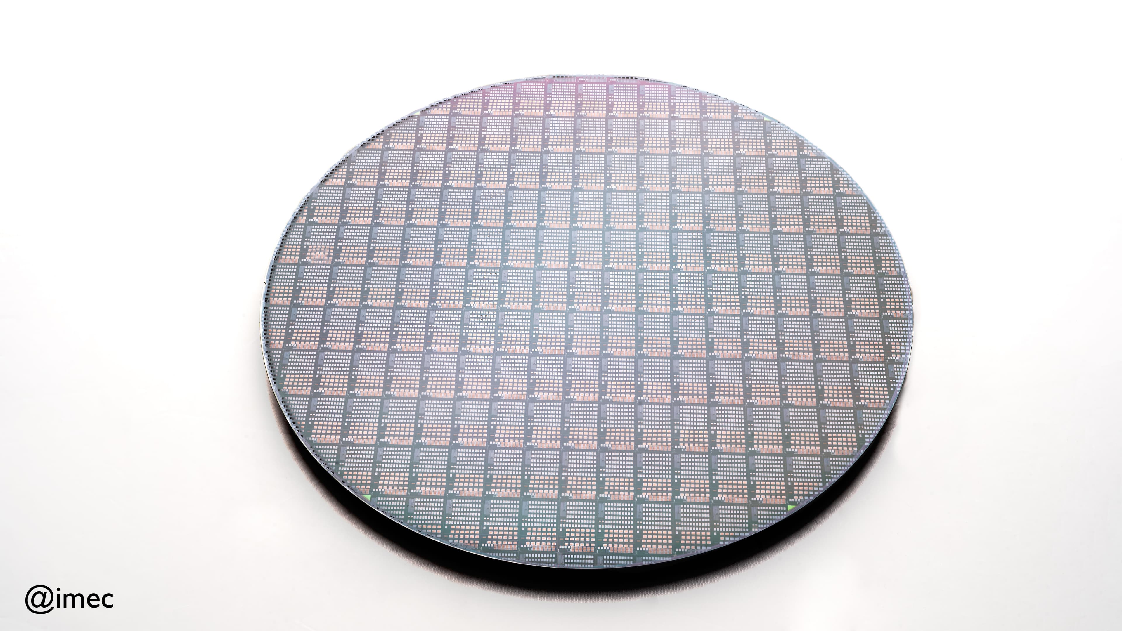
A 300mm silicon photonics wafer with flip-chipped InP laser diodes. Credit: Imec
Up to the job
Historically, optical communication links have gotten increasingly shorter, going from linking continents to homes and offices to servers within data centers. They’ll get shorter still, in the 1-10 centimeter range, as electrical connections between chips are starting to run out of steam.
Right now, this matter is most pressing at the high end of high-performance compute applications. Nvidia’s ‘data-center-in-a-box,’ for example, combines eight powerful GPUs with a massive amount of memory to handle demanding machine learning and data science workloads. The performance of this system hinges on processors and memory being able to exchange data swiftly and efficiently. Extrapolating current electrical interconnect speeds, they’ll become a bottleneck in two or three generations, Van Campenhout estimates.
Van Campenhout has been the director of imec’s Optical I/O R&D program since 2014. Over the past decade, his research focus leaned towards datacom and telecom applications, but recently, industry interest in short-reach optical interconnects has been accelerating dramatically, he says. “A number of companies, including several well-capitalized startups, are looking to aggressively deploy deeply integrated, short-reach optical interconnects to boost the performance of their high-performance compute systems.”
Imec’s integrated photonics activities
Next to its optical I/O R&D program and SiPh/SiN prototyping services at its home base in Leuven, imec is initiating a number of application-oriented silicon photonics activities in the Netherlands. Co-funded by the National Growth Fund, and working with TNO and other partners from the Photondelta ecosystem, the collaboration will focus on lidar and laser design at Holst Centre in Eindhoven and on agrifood applications at OnePlanet in Wageningen.
“It’s fabulous to see the investments by the Dutch Ministry of Economic Affairs with the National Growth Fund Photondelta. This financial impulse is critical since this industry is very much in the investment stage all over the planet. In addition, these funding mechanisms also nurture collaboration. Photondelta provides an excellent opportunity to strengthen cooperation within Holst Centre, both with local partners and across the border,” comments Kathleen Philips, vice president R&D at imec and general manager imec at Holst Centre.
“At imec NL, we focus on the design of more complete photonic systems, including the electronics and algorithms. By not only innovating on the building blocks, we specifically aim to create differentiating IP by connecting the various disciplines. The application domains are agrifood and health, as well as datacom and automotive lidar. Furthermore, the new system design activities at Holst Centre create a bridge between our long-standing photonics technology activities in Belgium and the photonics application research in OnePlanet, Gelderland.”
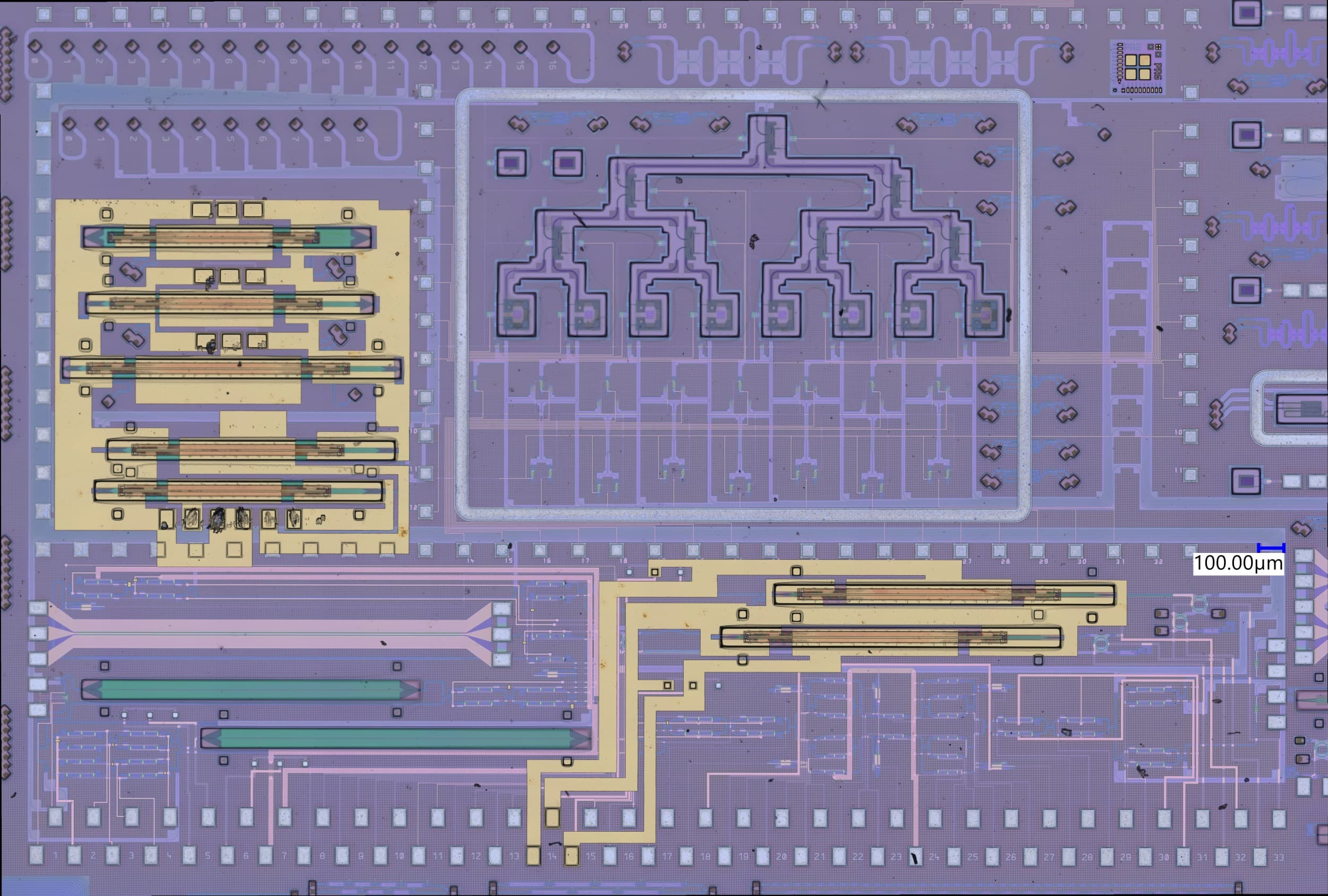
A silicon photonics test chip for solid-state lidar. Credit: imec
Down the road, this technology might trickle down to more generic applications. Leading-edge chip manufacturers, for example, are very serious about ‘partitioning’ their chips into multiple ICs, each with specialized functionality (CPU, I/O, cache memory, and so on). Especially over the relatively long distances within this context, copper wires might not be up to the job of interconnecting these chiplets.
That would require further improvements in bandwidth and power efficiency. In imec’s roadmap, the goal is to double the bandwidth and halve the power per bit of the optical subsystem every two years. As Van Campenhout already explained, that will require the introduction of new materials that might ‘break’ CMOS compatibility. But if there ever was a business case to take on that challenge, it’s probably inter-chip optical interconnects. “It’s going to be an exciting journey,” Van Campenhout says.
This article was first published in Bits&Chips and written in close collaboration with PhotonDelta.

Joris Van Campenhout is fellow silicon photonics and director of the industry-affiliation R&D program on optical I/O at imec. By advancing silicon photonics technology, imec’s optical I/O R&D program seeks to substantially scale optical interconnects to bandwidth densities beyond 1Tbps/mm, while consuming less power than 1pJ/bit, thereby enabling next-generation AI, HPC and cloud datacenter systems. Prior to joining imec in 2010, Joris was a post-doctoral researcher at IBM’s TJ Watson Research Center (USA), where he developed silicon electro-optic switches, and he obtained a PhD degree in Electrical Engineering from Ghent University (Belgium) in 2007, for his work on heterogeneous integration of InP microdisk lasers on silicon. Joris has authored or co-authored 15 patents and over 100 papers in the field of silicon integrated photonics, which have received 12,000+ citations.

Dr. Kathleen Philips is VP R&D and General Manager of imec Netherlands within Holst Center. She has been promoted in electrical engineering, is author and co-author of more than 60 papers and holds several patents. Philips joined imec in 2007 where she was chief scientist and led leading research programs in the field of Internet of Things. Before imec she was a scientist at Philips Research for over 12 years.
Published on:
3 January 2023


