This article was originally published in Chip Scale Review – Nov/Dec 2024
In this article we focus on the optical interfacing challenges for high-density co-packaged optics (CPO) applications, where assembly yield and scalability are added to the well-known requirements of low-loss, broadband, and polarization-independent optical coupling. Although efficient fiber-edge coupling to lensed fibers has been demonstrated using tapered Si mode-size converters in the 220nm-thick crystalline Si layer of the silicon-on-insulator (SOI) platform, the tight alignment tolerance because of the small spot size at the optical interface, along with the need for an air gap for the lensed fibers to function, prevents large-scale adoption for high-throughput packaging.
To engineer the optical interface for an increased spot size, the most common approach today is to use the SiN layers commonly found in the back-end-of-line (BEOL) stack of a complementary metal-oxide semiconductor (CMOS) chip. An inverse SiN taper is employed to transition the large optical mode from flat-cleaved, industry-standard single-mode fibers (SMF), to the tightly-confined mode in Si nano-waveguides, without sacrificing the simplicity of BEOL integration.
Edge couplers based on a hybrid platform consisting of a Si photonic layer combined with an additional SiN photonic layer offer typical coupling efficiencies to SMF of -1.5dB/fiber for both transverse electric (TE) and transverse magnetic (TM) polarization in O- and C-bands [1]. A critical aspect to these efficient edge couplers is the removal of the substrate below the buried oxide (BOX) layer of the SOI wafer to prevent the expanded mode from leaking into the Si substrate. While this enables the integration of V-grooves for passive assembly of SMFs, it places a constraint on the optical I/O density.
In order for CPO to deliver on its promise of high-bandwidth, low-latency, and low-power interconnects between compute chips (XPU) and high-bandwidth memory (HBM) in multi-node artificial intelligence/machine learning (AI/ML) clusters, a more scalable solution for optical interfacing is essential. At imec, several building blocks are being developed to enable this. One key building block involves further engineering the SiN edge coupler to achieve adiabatic mode conversion to high-density polymer optical waveguides [2]. This component serves as a mode converter to SMF while also providing optical redistribution capabilities on the interposer or package substrate. The solution increases the density of optical I/O connections and allows for higher fiber counts by relocating the fiber interface to the edge of the interposer or package, where more space is available.
A second building block leverages low-loss, high-density on-wafer SiN waveguides as wafer-level optical interconnects (WL-OI) between several tens of XPUs or HBMs [3]. This approach requires low-loss, high-yield optical coupling interfaces between the active photonic integrated circuit (PIC) dies and the optical interconnect wafer, where active PIC dies include the modulators and photodetectors, and the optical interconnect wafer includes the long-range routing waveguides and fiber coupling interfaces [4].
Optical redistribution layer based on polymer waveguides
The following sections describe the steps needed to design, fabricate, and characterize an optical redistribution layer based on polymer waveguides.
Design. Our first building block is based on adiabatic mode-conversion between silicon photonic chips with novel SiN tapers and a polymer waveguide (PWG)-based optical redistribution layer (optical RDL), which has the potential to be integrated on various types of interposer or package substrates.
For the optical RDL, several polymer optical waveguide materials are commercially available, offering excellent properties such as low optical loss, refractive index controllability, high-temperature stability, compatibility with reflow soldering, and stable optical properties. We selected two different polymer waveguide materials, EpoCore/EpoClad and OrmoCore/OrmoClad, both supplied by micro resist technology (Germany). For both materials, we studied two interfaces: 1) The SiN-to-PWG interface, and 2) The PWG-to-SMF interface. In both cases, the polymer waveguide dimensions were adjusted to optimize coupling efficiency, and ultimately, the dimensions were finalized for one material, which was later used in the experimental work.
The SiN tapered waveguides have a fixed height of 400nm, while the width varies along the taper, starting from the standard width of 710nm and narrowing to 130nm at the taper tip. The SiN is surrounded by a stack of multiple oxide layers to ensure mode confinement. For adiabatic coupling to occur, the optical mode should transfer from one waveguide to another with minimal conversion to radiation modes or higher-order modes. To achieve this, the SiN taper width must vary along the propagation direction in a carefully-engineered manner. The simplest option is to vary the taper width linearly along the propagation direction, allowing mode coupling to occur around the phase-matching point of the two waveguides. Although this is not the most efficient method for designing a taper coupler and generally results in longer tapers, we chose this approach to compare the performance of the two polymer waveguide materials.
The results of the EigenMode Expansion (EME) simulations are summarized in Figure 1 for EpoCore/EpoClad, and in Figure 2 for OrmoCore/OrmoClad. The higher refractive index contrast of OrmoCore/OrmoClad allows for the use of shorter SiN tapers, which is preferred. Because the ORDL needs to be coupled to SMF, the ORDL-to-SMF interface was also studied for both polymer waveguide materials, with varying waveguide dimensions. The results are summarized in Figure 3.

Figure 1: Coupling efficiency for SiN-to-ORDL adiabatic coupling as a function of the length of a linear SiN taper for various dimensions of a square EpoCore/EpoClad polymer waveguidbased ORDL.

Figure 2: Coupling efficiency for SiN-to-ORDL adiabatic coupling as a function of the length of a linear SiN taper for various dimensions of a square OrmoCore/OrmoClad polymer waveguidbased ORDL.

Figure 3: Overlap between the modes of a standard SMF and square polymer waveguides with varying dimensions.
For EpoCore/EpoClad polymer waveguides with dimensions between 3 and 6μm, an overlap efficiency of around 95% is achieved. Because of the larger refractive index contrast of OrmoCore/OrmoClad waveguides, the overlap decreases from approximately 83% for 6μm, to less than 70% for 3μm. For waveguides with dimensions below 3μm, the mode begins to expand due to reduced confinement. Although both polymer waveguide materials are viable based on this study, we decided to continue with EpoCore/EpoClad for further optimization of the SiN taper shape and for the experimental work.
For the optimization of the SiN-to-ORDL coupling interface, more efficient tapers have been designed by varying the taper width more rapidly in regions away from the phase-matching conditions, while varying the taper width more gradually in the critical regions where the optical mode is coupled. These critical regions are sensitive to size variations, and any rapid changes in taper size result in inefficient mode coupling, leading to increased radiation loss or coupling to higher-order modes. The exact layout of the SiN taper is defined using a semi-analytical method, ensuring a large overlap between consecutive sections of the taper [5]. EME simulations were used to optimize the SiN-to-ORDL coupler loss as a function of taper length, for wavelengths spanning the entire O-band. Designs with coupler lengths below 1mm, while maintaining a coupler loss well below 1dB for both polarizations across the entire O-band spectrum, have been achieved (results shown in Figure 4).
When investigating the tolerance for aligning the ORDL with respect to the PIC, we found a 1dB lateral misalignment tolerance of ±1.8μm, which is well within the capabilities of our target integration and assembly tools. The results are shown in Figure 5.

Figure 4: Broadband behavior of the SiN-to-ORDL adiabatic coupler, which is based on an EpoCore/EpoClad polymer waveguide.

Figure 5: Alignment tolerance of the ORDL with respect to the SiN tapered waveguide.
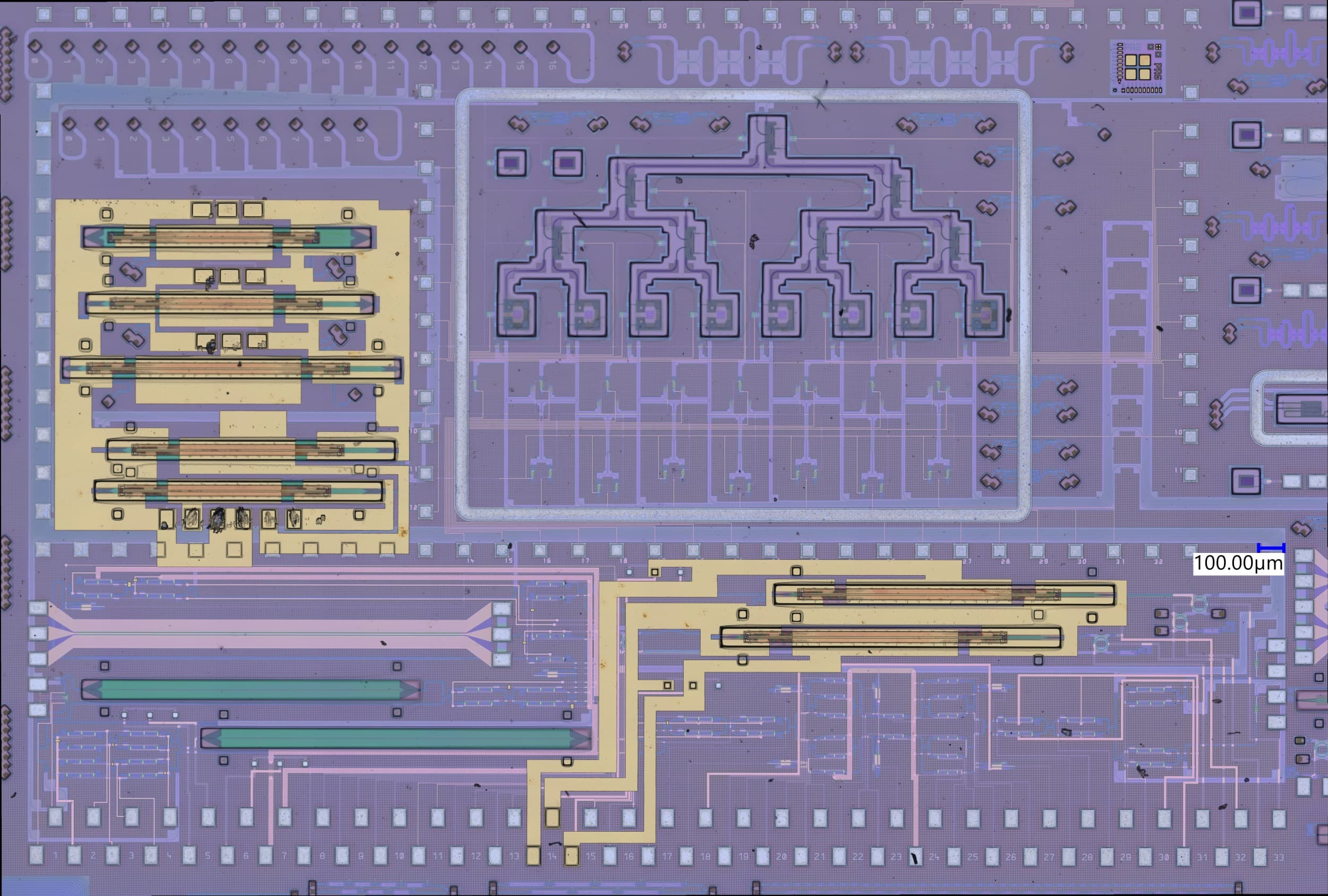
Fabrication. PICs with optimized SiN taper designs have been fabricated, and EpoCore/EpoClad polymer waveguides have been experimentally integrated by spin-coating the EpoCore material and lithographically patterning the polymer waveguides on the PIC. Both the spin-coating parameters and the lithographic patterning recipe have been iteratively fine-tuned to match the designed ORDL core dimensions. Figure 6 shows a fabricated test sample. In the final step, EpoClad is spin-coated to obtain a top cladding layer, ensuring that light is confined within the ORDL.

Figure 6: Optical microscope image of the ORDL integrated on PICs with SiN tapers.
Characterization. We prepared different test samples for optical characterization to allow for a breakdown of the total measured loss. For the ORDL cut-back analysis, polymer waveguides of varying lengths were used (without coupling to SiN tapers), and the propagation loss for the entire O-band was investigated.
At a wavelength of 1310nm, the propagation loss is below 0.5dB/cm. Additionally, a fiber-to-ORDL butt coupling loss of 1dB per facet was observed. The SiN test chips included SiN spirals to examine the propagation losses of the SiN waveguides. A loss of less than 1dB/cm was measured, which aligns with previously reported values for plasma-enhanced chemical vapor deposition (PECVD) SiN. A total fiber-to-fiber insertion loss of 4dB was experimentally measured, broken down into two 1dB fiber-to-ORDL coupling losses, 0.5dB of polymer waveguide propagation loss (for a 1cm waveguide length), 0.5dB of SiN waveguide propagation loss, and two 0.5dB losses per adiabatic transition between SiN and ORDL. Characterization results are summarized in Figure 7. Next steps will include implementing optical fan out within the ORDL and integrating optical RDL with electrical RDL on various types of interposer or package substrates.

Figure 7: characterization results following the integration of the optical RDL on PICs with optimized SiN tapers.
Wafer-level optical interconnects
The next building block under development is wafer-level optical interconnects. As interconnect distances are expected to reach several tens of centimeters, there is a strong need for ultra-low loss waveguides (<0.2dBcm) that can traverse the entire 300mm wafer, along with a sufficiently dense waveguide pitch (<10μm) and a sufficiently tight bending radius (<100μm). In this article, we present a 300mm wafer-scale SiN waveguide technology that combines low-pressure chemical vapor deposition (LPCVD) SiN waveguides with high-precision photolithographic reticle stitching, resulting in stitching losses below 0.01dB. In combination with the low linear propagation loss and the high optical confinement of the 400nm-thick LPCVD SiN waveguides, cross-wafer loop-back waveguides up to 56cm long are demonstrated, with an all-in waveguide loss of just 0.15dB/cm including up to 20 stitch interfaces as well as 56 100μm radius 90-degree bends.
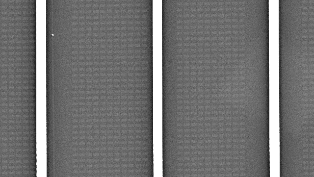
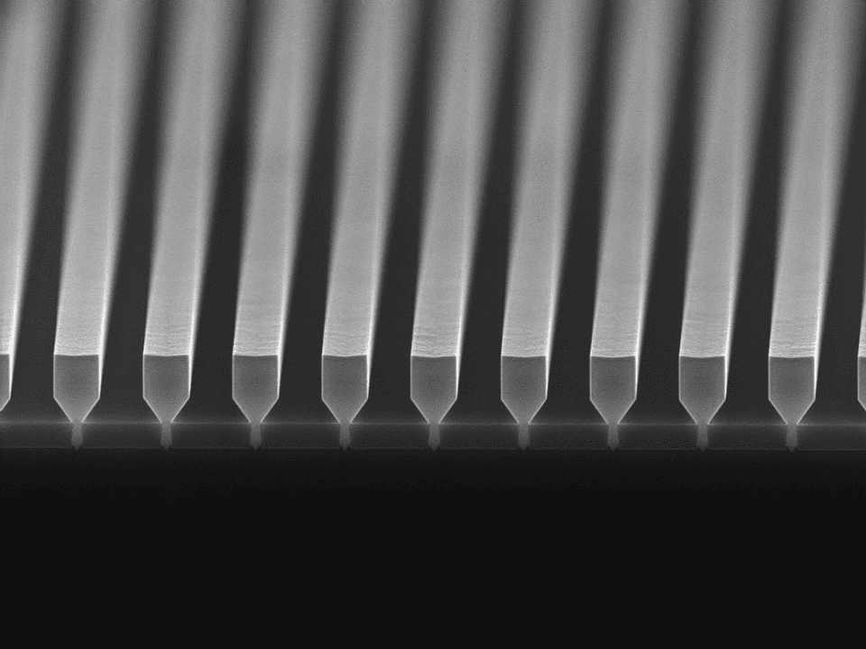
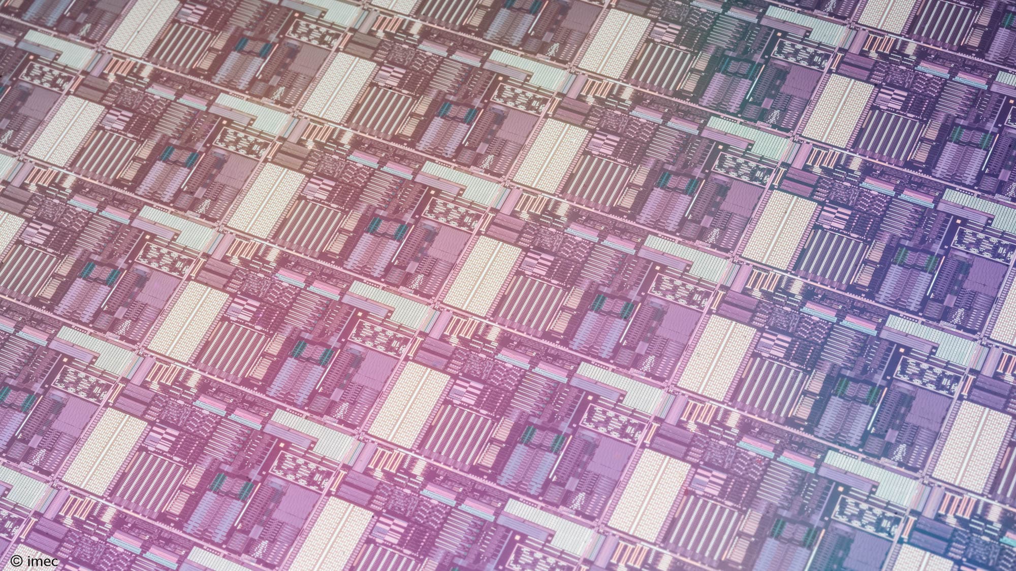
Wafer fabrication and reticle stitching. The 300mm wafer processing begins with the deposition of a 2.7μm-thick silicon oxide layer. Next, a 400nm-thick LPCVD SiN layer is deposited. The LPCVD SiN layer is patterned using 193nm immersion lithography with two different reticles, each covering a full 26mm x 33mm die. Each die is exposed with the chosen reticle via a dedicated photolithography job, resulting in the complete wafer exposure, as shown in Figure 8a. To enable reticle stitching between neighboring dies, each die overlaps with all adjacent dies, and overlay structures are placed in this overlap to characterize die-to-die misalignment. Several scanning electron microscope (SEM) micrographs of the stitching interfaces are shown in Figure 8b, revealing a very smooth transition without any significant waveguide shape irregularity. The misalignment between neighboring dies was measured using dedicated overlay marks at six separate locations per die. A full-wafer measurement was carried out on a total of four wafers, and the maximum observed x- or y- misalignment was 12nm. After the SiN patterning, an oxide top cladding layer is deposited and subsequently planarized, targeting 2.6μm of remaining oxide on top of the SiN.

Figure 8: a) Photograph of a fabricated 300mm wafer with reticle-stitched SiN waveguide bundles; and b)dtailed top-view SEM images of the stitched regions.
Design of the stitching interface and optical test structures. Leveraging the high alignment accuracy of reticle stitching with advanced 193nm lithography, as described in the previous section, we designed relatively simple, abrupt stitch interfaces with a compact footprint. Two key design parameters were explored to target low optical loss for TE modes in the O-band: 1) the waveguide width at the stitch interface, optionally tapering up to 1.8μm or 2.5μm from the nominal 710nm SiN waveguide width (using compact low-loss tapers with length below 35μm); and 2) the overlap between the two lithographic exposures, ranging from 10nm to 50nm. According to full 3D finite-difference time-domain (FDTD) simulations, such interfaces are expected to yield optical loss below 0.006dB for overlay errors up to 20nm. Dedicated spiral waveguide structures with 100 stitching interfaces were implemented, along with a reference spiral waveguide without stitching, to extract the stitching loss at the wafer scale.
As a simple proof-of-concept demonstrator, we also included several cross-wafer loop-back waveguides by arranging waveguide bundles (on the first reticle) and bending/termination structures (on the second reticle). The loop-back waveguides feature varying total propagation lengths (up to 56cm), number of stitching interfaces (up to 20) and counts of 100μm radius 90-degree bends (up to 56), all designed with the same stitching taper-width design sweep. For all test structures, SiN grating couplers were implemented to perform wafer-scale testing.
Measurement results. First, SiN waveguide loss and bending loss measurements were carried out using standard test structures consisting of cut-back spiral waveguides with 50μm radius 90-degree bends, revealing a nominal linear propagation loss of 0.165dB/cm and bending losses of 0.007dB/bend (Figure 9a). Next, the stitched spiral test structures were measured. The extracted stitching loss values are generally very low (Figure 9b), with some cases showing negative values due to imperfect fiber coupling repeatability during wafer-scale testing (~1dB variability). Therefore, we can conservatively derive the upper limit for the stitching loss to be 0.01dB/interface.
Subsequently, the cross-wafer loop-back waveguides were measured, as shown in Figure 9c. The extracted all-in (length-referred) waveguide loss was derived from linear fitting to be 0.15dB/cm for all sets of loop-back waveguides measured on the wafer, independent of the stitching taper width. Even the non-tapered SiN waveguide with a width of 710nm exhibited such low stitching loss, further confirming the high alignment accuracy during lithography. Additionally, the demonstrated taper-less stitching interface has the smallest possible footprint.

Figure 9: a)SiN waveguide propagation loss and 90-degree bend from spiral waveguides on standard test structures across the water; b) Measured stitching loss from test structures vs. lithography overlap and taper width; and c) Measured fiber-to-fiber insertion spactra from cross-water loop-back SoiN waveguides and linear fitted all-in waveguide loss spectrum (in red).
Optically interconnected system-on-wafer
A high-precision collective die-to-wafer dielectric bonding process is utilized to allow for low-loss SiN waveguide-based evanescent coupling between the assembled PIC dies and the 300mm optical interconnect wafer (Figure 10b). Tapered SiN waveguides, specifically designed for efficient, alignment-error tolerant, and broadband evanescent coupling, consistently yield insertion losses below 0.5dB in the O-band for evanescent couplers (EVC) as short as 0.5mm.
Wafer fabrication, collective die-to-wafer assembly and SiN EVC design. The 300mm wafer processing begins with a 4.1μm-thick silicon oxide deposition, which serves as a bottom cladding layer and reduces the interaction of the evanescent coupler (EVC) mode with the Si substrate. Next, a 400nm-thick PECVD SiN layer is deposited and patterned using 193nm immersion lithography. After the SiN layer is patterned, an oxide top cladding layer is deposited and subsequently planarized—targeting 200nm of remaining oxide on top of the SiN. A thin SiCN layer is then deposited to enhance the collective die-to-wafer bonding strength. Subsequently, the assembly process starts by flipping and bonding the wafer to a first temporary carrier, to thin the Si substrate down to 100μm. Next, the 7x7mm2-sized dummy “active” PIC dies are singulated using blade dicing. The PIC dies are then placed and aligned using primary alignment marks on a second temporary glass carrier. Finally, the PIC dies on the glass carrier are collectively transferred to the bottom PIC wafer and again aligned, using secondary overlay markers. A schematic view of the resulting cross section is shown in Figure 10c. Figure 10d shows a TEM image, illustrating the two SiN EVCs separated by the 400nm-thick oxide cladding and 30nm-thick SiCN dielectric bonding layer.

Figure 10: a) Schematic view of an optically-interconnected wafer-scale system leveraging EVCs for low-loss coupling between the active PICs and passive interconnect wafer; b) Simplified collective die-to-wafer assembled photonic system reported in this article; c) Detailed schematic cross-section of the assembly and EVC stack; and d) cross-section TEM image of the collective die-to-wafer bonded SiN-based EVC.
Multiple design approaches exist to optimize the adiabatic SiN EVCs for achieving broadband, low-loss coupling and robustness against alignment errors. In this work, we have adopted the “FAQUAD” (fast quasi-adiabatic) method [6], resulting in a typical EVC profile as depicted in Figure 11c, which tapers the SiN waveguide width from a nominal 710nm down to a minimum of 130nm in the EVC region. EVC lengths of 0.5mm, 1mm and 1.5mm have been implemented to explore the trade-off between coupler footprint, coupling performance, and robustness against misalignment. Of the 100 PICs bonded to the wafer, as shown in Figure 11a, 51 of them contain the FAQUAD EVCs, which we will report on in the remainder of this article. The other 49 bonded PICs contain alternative EVC designs that will be reported elsewhere. To extract the EVC loss, three test structures with varying number of EVC transitions (0, 6 and 18) are implemented and measured at wafer scale using SiN fiber grating couplers (Figure 11d-f), using TE polarized laser light in the O-band. A bivariate linear fit is applied to decouple the SiN EVC from the SiN waveguide loss (Figure 11f-i).

Figure 11: a) Photograph of a 300mm optical interconnect wafer assembled PIC dies; b) Overall layout of the bottom wafer and top PIC; c) "FAQUAD" taper profile used for the SiN waveguide EVC; d) EVC loss test macro; e) x-y alignment definition; f) Typical measured fiber-to-fiber transmission spectrum; g) Bivariate fitting procedure to extract EVC and waveguide loss; and h) Typical extracted EVC and waveguide loss spectra.
Wafer-scale measurement and analysis of SiN EVC loss. Using the test structures described above, we conducted wafer-scale measurements of the EVCs of varying lengths. Figure 12a shows the resulting EVC loss spectra across 60nm of the O-band. At a wavelength of 1310nm, the majority of EVCs have extracted insertion losses below 0.5dB (see Figure 12b), with mean ±3σ values of 0.36±0.18dB, 0.37±0.24dB, and 0.32±0.15dB for the 1.5mm, 1mm and 0.5mm-long EVCs, respectively. At shorter wavelengths, several dies exhibit higher EVC loss, primarily occurring in PIC dies with larger lateral (y) misalignment. It is important to note that the SiN waveguide propagation loss on the reported wafer (and top PIC dies) is relatively high, ranging from 4 to 6dB/cm due to a processing issue. Part of this excess propagation loss is also embedded in the extracted EVC loss, and by reducing this propagation loss in future experiments, we expect to be able to reduce the EVC loss by 0.1 to 0.2dB.
In terms of overall optical yield, the 1.5mm-long EVC design performs best at 75.5%, followed by the 1mm and the 0.5mm-long EVC at 68% and 57%, respectively. The imperfect yield obtained in this initial development run is caused by several factors, including die loss during the collective die-to-wafer assembly process, the formation of undesired voids (mostly appearing at the die edges), and lateral (y-axis) misalignment. The 0.5mm-long EVCs are particularly sensitive to lateral misalignment, as shown in the left panel of Figure 12c, where 7 dies with non-functional EVCs exhibited a lateral misalignment greater than 1μm. The 1.5mm-long EVC can tolerate up to 1.5μm of lateral misalignment, as illustrated in the right panel of Figure 12c. As expected, longitudinal (x-axis) misalignment has a much less pronounced effect on coupling loss. All factors contributing to yield loss are being addressed by optimizing the collective die-to-wafer bonding process, and results will be reported in future work.

Figure12: Wafer scale EVC loss measurements vs. coupler length; a) Loss spectra; b) loss statistics at 1310nm wavelength; and c)Loss vs. x- and y misalignment.
Note: dData points without color represent non-functional EVCs.
Acknowledgments
This work was supported by imec’s industry-affiliation R&D program “Optical I/O,” and by the European Union’s Horizon Europe Research and Innovation Program under Agreement 101070560 (PUNCH). The authors would like to acknowledge all team members who contributed to the work and assisted in writing the ECTC and OFC conference proceedings, upon which this article is largely based (references [2], [3], and [4]).
References
[1] F. J. Ferraro, et al., “Imec silicon photonics platforms: performance overview and roadmap,” Proc. SPIE 12429, Next-Generation Optical Communication: Components, Sub-Systems, and Systems XII, 1242909 (2023).
[2] G. Van Steenberge, et al., "Interfacing silicon photonics for CPO," 2024 IEEE 74th Electronic Components and Tech. Conf. (ECTC), Denver, CO, USA, 2024, pp. 1161-1165.
[3] P. Xu, et al., "Low-loss, multi-reticle stitched SiN waveguides for 300mm wafer-level optical interconnects,” Optical Fiber Communication Conference (OFC) 2024, Technical Digest Series (Optica Publishing Group, 2024), paper M4A.3.
[4] P. Xu, et al., "Collective die-to-wafer bonding enabling low-loss evanescent coupling for optically interconnected System-on-Wafer," 2024 Optical Fiber Communications Conf. and Exhibition (OFC), San Diego, CA, USA, 2024, pp. 1-3.
[5] J. Van Asch, et al., “A methodical approach to design adiabatic waveguide couplers for heterogeneous integrated photonics,” J. Phys. Photonics 6 045013 (2024).
[6] D. Siriani, and J.L. Tambasco, "Adiabatic guided wave optics – a toolbox of generalized design and optimization methods," Opt. Express 29, 3243-3257 (2021).
With over 20 years of experience in advanced integration and photonics packaging technologies, he is an IEEE Senior Member and has (co-)authored 65 peer-reviewed articles and more than 145 conference papers. He also holds 14 granted or filed patents. Additionally, he chairs the IOF Business Development Center e-Poly at Ghent U. Email: geert.vansteenberge@ugent.be
Published on:
26 November 2024


