For each solar cell semiconductor material, there is an intrinsic limit to how much light can be converted into electricity. For silicon PV technology, for example, that limit is around 30%, and the industrial solar panels are now reaching results that are plateauing some 10% below this limit. From now on, additional gains will be small and not so easy to attain.
Therefore there is a growing interest in tandem cells, solar cells that are made by stacking two or more cells on top of each other to reach a power conversion efficiency that is higher than what would be possible with the separate technologies. An obvious requirement is that the material of the top cell is transparent to the light that it doesn’t convert. An additional boost is given if the materials in the stack are sensitive to a distinct part of the light spectrum, so that they don’t scavenge on each other’s conversion potential. The material that captures the shortest wavelengths (e.g. blue and green) will then be on top, while the bottom material converts the longer wavelengths (e.g. red and near-infrared).
Tandem cells, or multi-junction cells as they are also called, were originally used for spacecraft, where expensive III-V materials such as gallium-arsenide (GaAs) or germanium (Ge) were first combined to reach higher efficiencies than what was possible with any single-junction cell. These cells, however, are much too expensive for terrestrial, large-scale use. To build cost-effective tandem cells, the most obvious way is to add a new material on top of today’s conventional mono-junction cells, which are either based on silicon or on a thin film material such as CIGS (copper indium gallium selenide).
A new, intriguing material
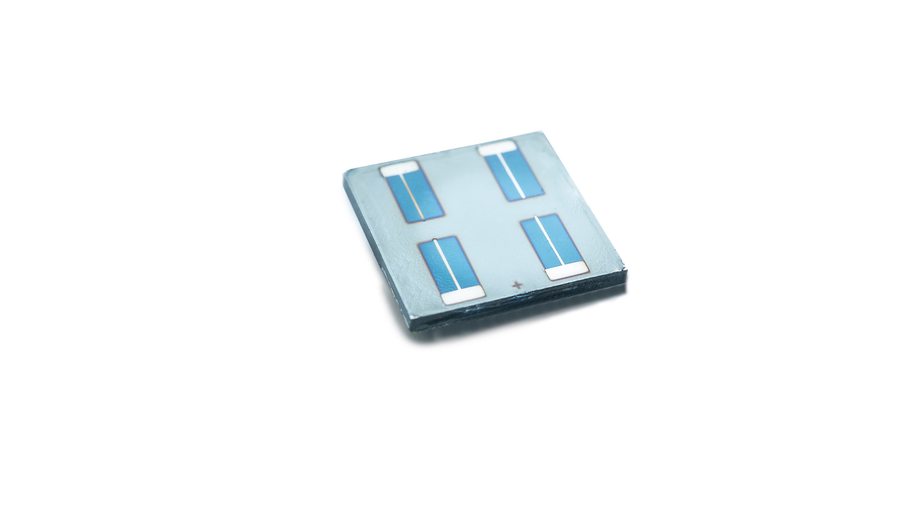
A low-cost candidate material for the top cells is perovskite, a material that only recently appeared on the PV technology radar. Perovskite is a family of materials that have been known for some time because of their intriguing physical properties. They have been studied e.g. as a piezoelectric material, as superconductors, or to catalyze chemical processes. And only as recently as 2009 also to convert light into electricity, integrated in a dye-sensitized solar cell architecture with a modest 3.8% conversion efficiency and a short lifetime. Since then, labs around the world have steadily improved the architecture, reliability and efficiency of perovskite solar cells, now above 22%.
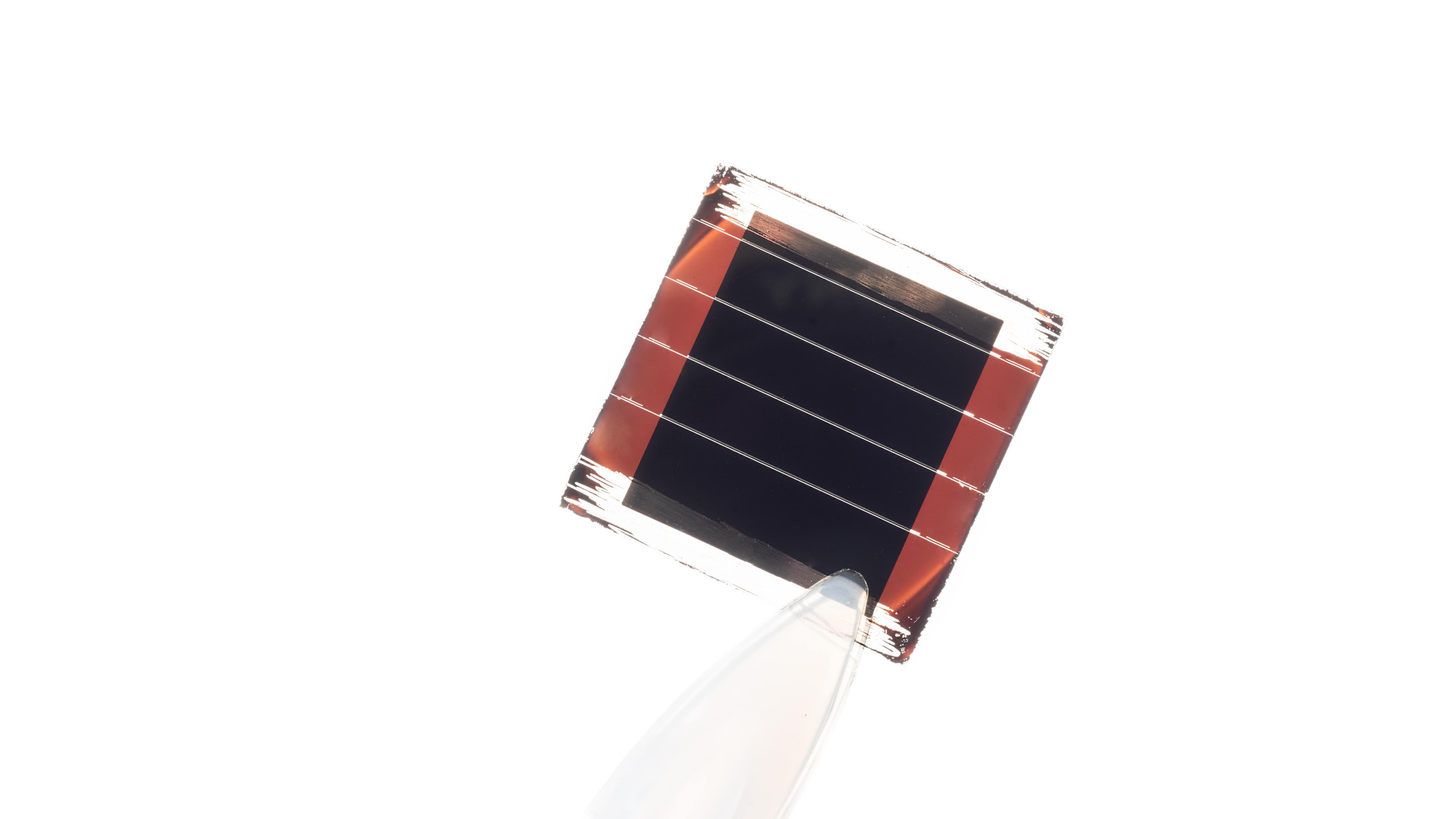
Perovskite solar cells have many desirable properties. They are potentially cheap to produce: they can be made with simple fabrication techniques such as coating and printing with ink-like materials. And they have a high absorption efficiency for sunlight, so not much of the material is needed, a layer of at most a few hundred nanometers. Moreover, the material can be carefully engineered to result in various optical and electronic properties, even transparent cells are possible.
Just what the experts were looking for as a top cell material: thin, transparent, cost-effective, tunable.
A turbo boost for silicon and CIGS
Imec’s researchers chose silicon and CIGS technologies – the most widely fabricated and installed PV technologies – to add a perovskite boost layer. An obvious choice, because imec has a decade long expertise with improving solar technology in an industrially relevant way and in collaboration with solar cell manufacturers.
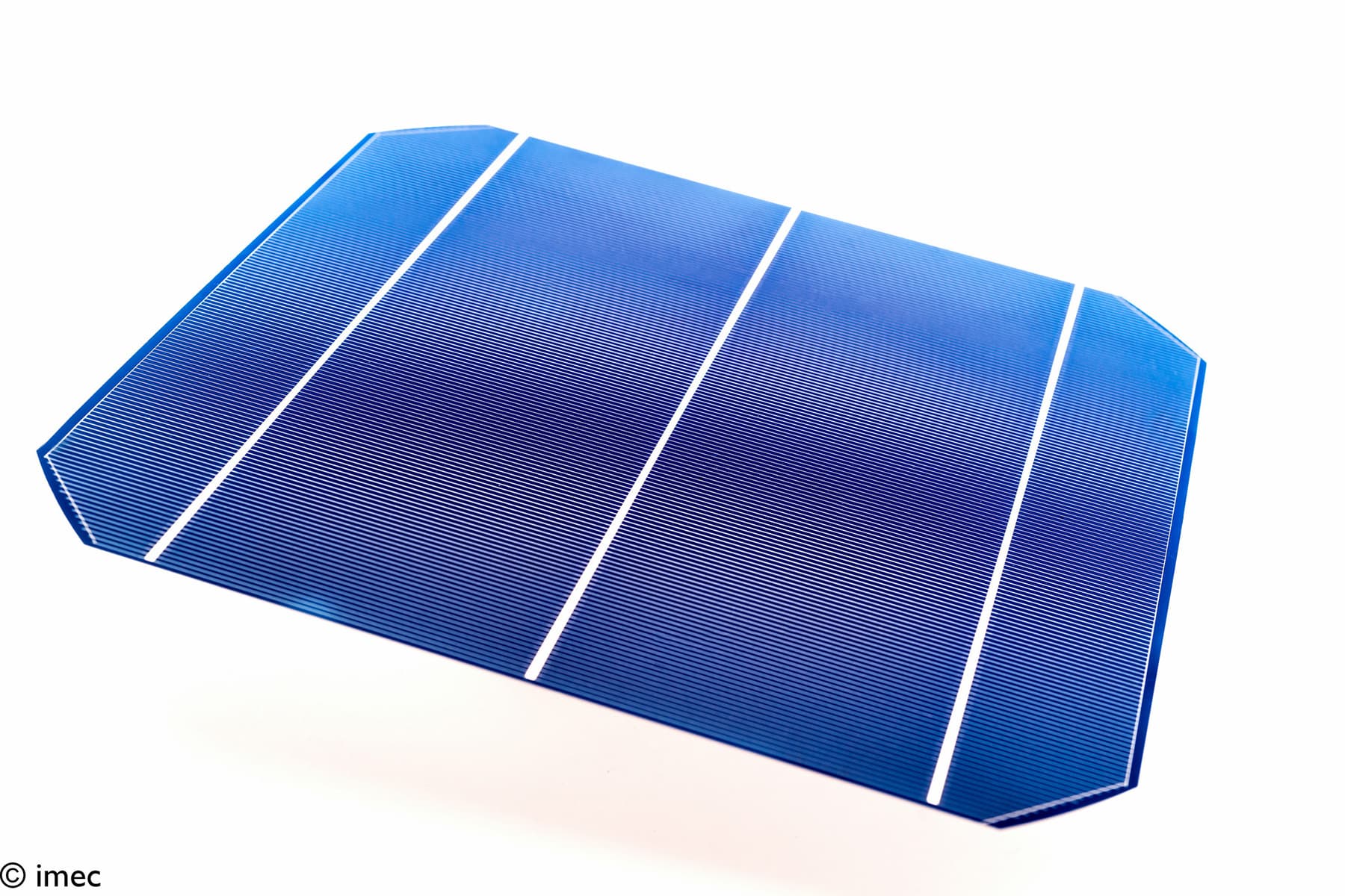
A first result was obtained by stacking a 0.13 cm² spin-coated perovskite cell stacked on top of a 4 cm² industrial silicon cell in a 4-terminal configuration (more about that later). The silicon cell used in this case has an IBC architecture (interdigitated back-contact), meaning that it has both contacts on the backside, leaving the front side on which the perovskite cell sits completely free to convert incoming light. With a power conversion efficiency of 27.1 percent, this tandem already beats the most efficient standalone silicon solar cell, with room for further gains.
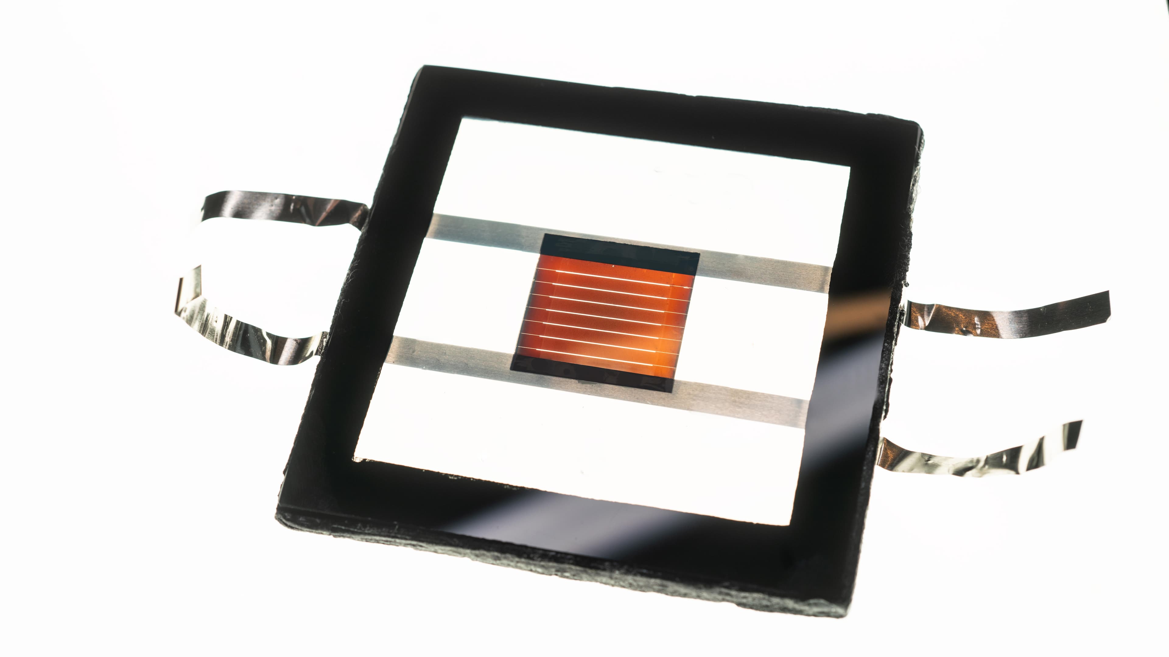
And a second record, 24.6%, was obtained again with a 0.13 cm² perovskite cell, but this time stacked on top of a 0.5 cm² CIGS module. This work was done in collaboration with one of the world-leaders in CIGS technology, the Zentrum für Solare Energiewirtschaft (ZSW, Stuttgart, Germany). This result beats that of last year’s demonstrator with a whopping 5%, showing the potential for improvement that can be made with tandem combinations like these. Compared to the previous year’s tandem, the translucence of the perovskite cell for near-infrared light was improved, and the perovskite material itself was engineered to have a better tandem efficiency.
A notable difference between imec’s two tandem cells is that unlike silicon technology, CIGS is a thin-film technology. That makes the perovskite-CIGS cell a full thin-film solution that can be fabricated on flexible foils. To be used for example in building-integrated PV applications.

Imec’s researchers chose silicon and CIGS technologies – the most widely fabricated and installed PV technologies – to add a perovskite boost layer. An obvious choice, because imec has a decade long expertise with improving solar technology in an industrially relevant way and in collaboration with solar cell manufacturers.
Not all roses and moonshine yet
These two top results not only proved the worth of perovskite as a top cell material, they also point to the fact that – because of its characteristics and flexibility – perovskite technology could be used to boost virtually any type of single-junction solar cell.
However, there are also a few challenges with the perovskite layer that still have to be solved before tandem cells can be fabricated commercially.
One is that the cells’ stability has not kept suit with the improving efficiency. Perovskite cells still degrade too quickly, lasting only weeks or months instead of years or decades. Innovative barrier and insulating layers have already much improved the cells’ stability, but there is still some way to go.
And a second issue is that all efficiency records were made on small-sized cells, sometimes measuring a mere square centimeter. The challenge is now to translate the excellent efficiencies to large cells, modules and eventually PV systems.
Unrelated to stability, but also essential, is the toxicity of the material. The perovskites that are used today include lead. And although the concentration in final PV systems will be very low, scientists are also looking at other solutions using tin (Sn) to arrive at sustainable PV technology and consumer products that adhere to the WEEE (Waste Electrical and Electronic Equipment) and RoHS (Restriction of Hazardous Substances) regulations.
On all these issues, we’re slowly progressing, carefully tuning the recipes and processing steps. This work is done in collaboration with a number of industrial partners. So in contrast to the more science-oriented initiatives, our effort is focused on developing industrially-suitable processes.
Two configurations with pros and cons
The tandem modules that imec initially designed and tested were so-called 4-terminal modules, with the two subcells of the tandem electrically isolated and each having their own wiring. As a result, the finished product has four electrical wires coming out and therefore requires an additional convertor. In a 2-terminal module, in contrast, the two subcells are electrically connected in series and the module has only two terminal wires, a simpler configuration that is next on imec’s optimization agenda.
With the added complexity, why go for a 4-terminal setup? Mainly because it allows getting the best out of the two subcells. With a 4-terminal setup, it pays to use the best, optimized single-junction cells as a subcell. A 2-terminal configuration, in contrast, comes with the constraint that the series connection requires the currents to match. This may eat into some of the edge of the subcells.
Overall, the difference in efficiency between 4-terminal and 2-terminal modules is only small when measured in the lab under standardized conditions. In the field, however, with light conditions that change from minute to minute, the 4-terminal architecture has the potential for a higher yield. The downside of course is the added cost for the separate wiring, convertors, junction boxes… Therefore, companies have shown much interest in the 2-terminal solution, which can be assembled into panels that can simply replace today’s panels without additional cost.
Adding perovskite on top of industrial silicon PV may prove to be the least costly approach to further improve the efficiency of photovoltaics. We therefore invite all companies in the PV value chain that are looking into higher efficiencies to partner with us and explore this promising path.

Manoj Jaysankar is a graduate of the Erasmus Mundus Master in Nanoscience and Nanotechnology (EMM-Nano) program where he specialized in nanoelectronics and earned a joint M. Sc. Degree from KU Leuven, Belgium and Chalmers University of Technology, Sweden. In December 2014, Manoj joined the photovoltaics department of imec as a doctoral researcher and is currently working towards a Ph.D. degree in association with KU Leuven, Belgium. His research focuses on design and development of high-efficiency, perovskite-based tandem solar cells. Email: manoj.jaysankar@imec.be
Published on:
1 October 2018


