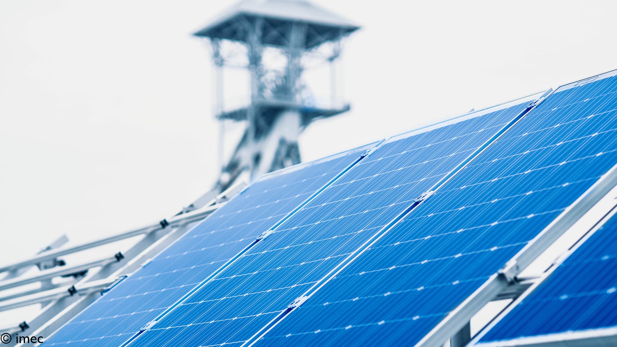
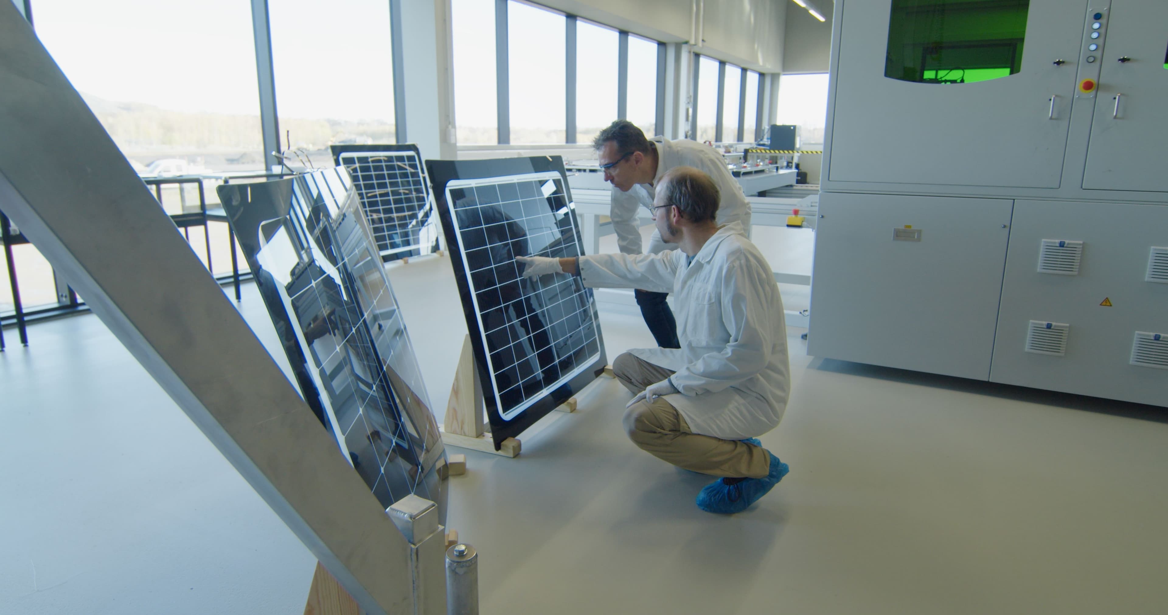
Thin-film PV technology has been around since the mid-20th Century (in solar-powered calculators, for example). They were rightly considered the lower-efficiency, yet cheaper, equivalent of conventional Si-PV for a long time. Meanwhile, thanks to multi-junction devices, their efficiencies are competing with (and at lab-scale even surpassing) those of Si-PV. For example, thin-film PV technologies, such as copper indium gallium diselenide (CIGS), have become an established solution in iconic buildings with building-integrated PV (BIPV). Over the past decades, imec has been a key player on the forefront of technology innovations that have brought thin-film PV to its current state-of-the-art and on the verge of conquering the market.

Thin-film PV is already being used for building-integrated PV in iconic buildings. Left: City of Music, Paris, Shigeru Ban architects, BIPV by ISSOL | Middle: French Ministry of Defense, Paris, ANMA architects, BIPV by ISSOL (©Agence Nicolas Michelin & Associes) |Right: Finance Tower, Liège BE, Jaspers Eyers architects, BIPV by ISSOL ©P.Andrianopoli (Pictures: Courtesy of ISSOL).
In terms of market share, the big breakthrough of thin-film PV has yet to happen but might be nearer than ever before because of the drive to near-zero-energy buildings and local energy communities. The last decade has brought numerous advances in thin-film R&D, allowing it to start proving its value on a larger scale, especially in integrated-PV solutions such as buildings, vehicles, agri-PV, and others. As a kind of paradox, the dominant Si-PV market might provide the ideal jumping board for thin-film to close in on the top position.
Combining the best of both worlds: Si-thin-film tandem devices
The PV-market has grown at a breathtaking rate over the last two decades resulting in a market size that is a thousand times larger than twenty years ago and reaching an installation volume of over 100GWp/year in 2019, which was equivalent to a yearly turnover in the range of $150B.
Although the exact growth scenario remains to be seen, there are sufficient elements to believe that, due to its cost-effectiveness and distributed character, further growth of the PV-sector by a factor of ten in the next two decades is highly probable. In this ambition, performance increase remains critical more than ever before. The present evolution of PV-system prices and their composition often results in an erroneous conclusion. Given that nowadays, the price components related to cell and module manufacturing no longer dominate the total cost, many conclude that it is no longer relevant to look at the PV-cell and module level. This conclusion is, however, totally incorrect. The best way to reduce the weight of all the peripheral and adjacent components such as wires, switches, inverters (aka balance-of-system, or BOS, components) is to increase the number of Wp/m2 or ultimately kWh/m2.
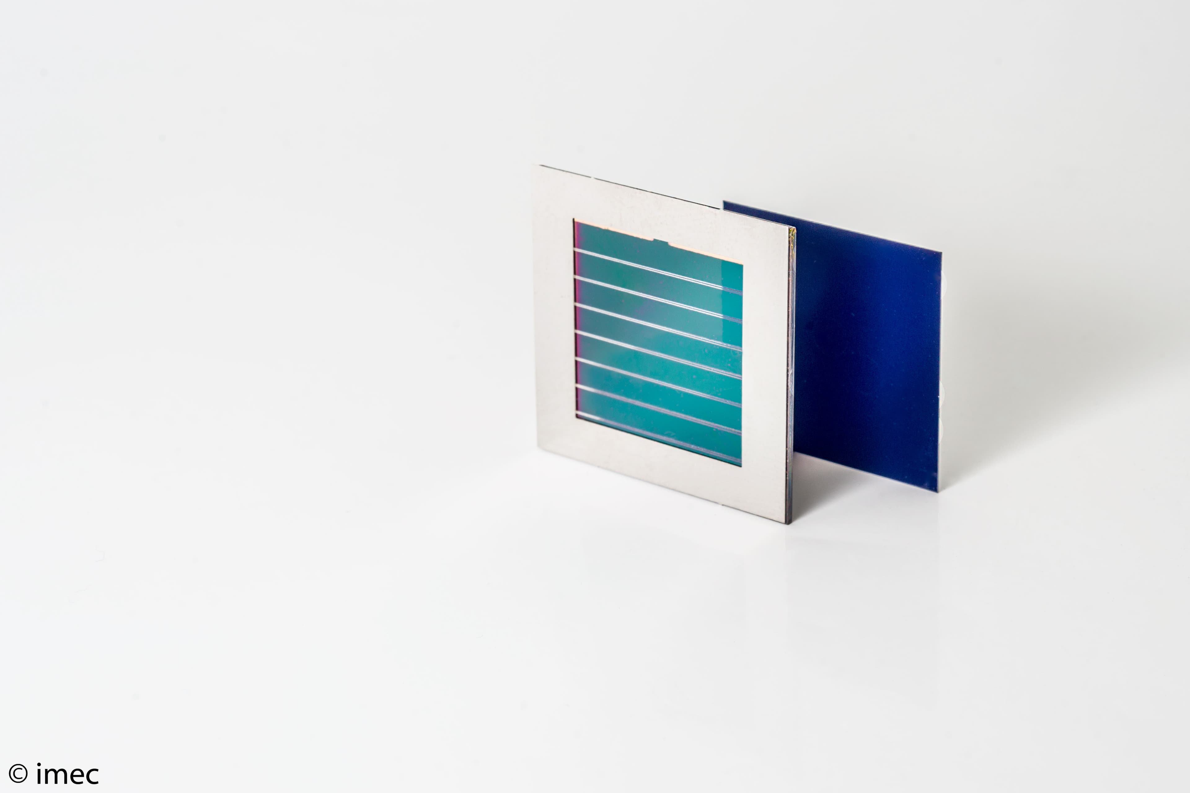
Multi-junction PV devices – in this case, a tandem cell of perovskite on top of Si – allow to optimally cover the solar spectrum and increase the energy conversion rates of the overall system.
Since crystalline Si-cells are approaching their practical limit in terms of energy conversion (implied by physical laws), the objective of a performance enhancement can only be achieved when moving towards tandem and ultimately triple-junction configurations; with the goal of going over the 30% limit and aim at 35% on cell level. In such multiple-junction systems, various electroactive materials are stacked that have complementary sensitivities within the solar spectrum. Combined, they make more optimal use of the available spectrum and thereby increase the conversion rate of the overall system.
The type and variety of available materials in thin-film PV allow for optimally tuning each subcell's bandgaps within the tandem, so they cover complementary parts of the solar spectrum. Also, thin-film solutions are lightweight, flexible, and relatively cheap to produce. Because of these inherent characteristics, thin-film technologies are ideally suited to act as the additional layers in traditional Si-PV stacks and, as such, augment them. By doing so, thin-film technologies can optimally take advantage of the existing market scale to further lower their production cost. Moreover, this economy of scale will help to develop the size of the niche markets for products that are purely based on thin-film PV (e.g., vehicle-integrated PV).
Opportunities for Europe
The largest part of the PV cell and PV module manufacturing capacity is presently located in Asia and concentrated in China and Malaysia. Although the heart of a PV ystem is obviously the PV cell, the PV module today represents less than 30% of the PV system's final value in the value chain. It’s important to emphasize that on materials level (encapsulants, glass, metals), balance-of-system (BOS) components, design, installation, operations and maintenance, decommissioning, and recycling/reuse… European companies take a significant part in value creation and are leaders in innovation.
The same holds for thin-film technologies, where tight collaborations within the value chain are even more critical because of the ambitions in terms of integration and mass-customization. Because thin-film technologies require tight integration with conventional PV processing or need to meet the customization requirements of specific end applications in terms of dimensions, shape, and transparency (think of integration in buildings), there will be enormous value in having a coherent production ecosystem as close as possible to the location where the final system needs to be applied. Be it a building-integrated solution (BIPV), in-vehicle integration (VIPV), or the like.
And it’s precisely on this aspect of tight collaboration and ecosystem coordination that Europe can deploy its proven strengths.

Building-integrated photovoltaics (BIPV) façade developed within the EU-funded project PVme.
Imec’s track record in thin-film PV
One of the proof points of Europe’s strength in R&D collaboration is Solliance, a Solar Research Alliance that since its foundation in 2010 (by TNO, ECN, Holst Centre, TU Eindhoven, and UHasselt) plays a leading role in the worldwide research and development of thin-film solar technology. Imec joined the Netherlands-based initiative as one of the pioneers shortly after the official start and has since worked closely with TNO and the Solliance academic partners to push the boundaries of thin-film PV. Another prime example is EnergyVille, a collaboration between the Belgian research partners KU Leuven, VITO, imec, and UHasselt in sustainable energy and intelligent energy systems. A brand-new lab for thin-film-PV development and upscaling was opened at the EnergyVille-site in 2018, which enormously increased the group's impact in paving the way to upscaling, PV-module making, and stability studies under controlled or outdoor conditions. The efforts on materials development and characterization at IMOMEC, an imec research laboratory at UHasselt, should also not be overlooked.
Together, these collaborations formed the solid foundation in a field that was substantially disrupted by the appearance of a new group of materials: perovskites.
Until a decade ago, one of the main activities in the thin-film R&D domain was on organic photovoltaics (OPV): thin-film technologies that use organic compounds as semiconductor material. Since then, perovskites – a specific group of hybrid organic-inorganic materials – have wholly disrupted the field and dominated the thin-film PV domain. They are by far the prime candidate to guarantee the basic efficienciy of thin-film solutions, be it still in combination with other materials such as CIGS to realize the beforementioned multi-junction devices.
Thanks to the available knowledge and collaborations named above, the move from OPV towards perovskites turned out to be particularly successful in terms of results obtained on upscaled devices. As it happened, the processing equipment and conditions required for perovskite-based systems were similar enough to the ones for OPV, allowing Solliance to build on two decades of R&D that imec and other partners had been building on OPV and other advanced thin-film PV technologies. For example, techniques such as spray coating and evaporation developed for OPV and other thin-film flavors proved to be compatible with perovskites after relatively minor tuning of the material stacks, equipment, and processing conditions.
As a result, imec/EnergyVille, together with the Dutch partners in the Solliance collaboration, achieved globally leading results, such as the world’s first officially certified large-area perovskite module and several world records in the energy efficiency of thin-film PV cells and systems. Aside from these efforts and achievements on materials and cells, imec and its partners also deploy activities on the adjacent competences. For example, at EnergyVille focus lies on the topics that are covering the entire value chain from material to (Integrated) PV system. Starting from the vision that Europe can differentiate itself in terms of customization, integration, and the related flexibility in manufacturing conditions, for example, research is conducted on dedicated interconnect solutions that allow for flexibly interconnecting individual (thin-film) PV cells into modules with a diversity of shapes and dimensions. Also, components and systems such as inverters and other peripheral electronics are being investigated in terms of how they can evolve to comply with the specific requirements of PV implementations with a higher degree of customization than what exists in today’s relatively standardized Si-PV implementations.
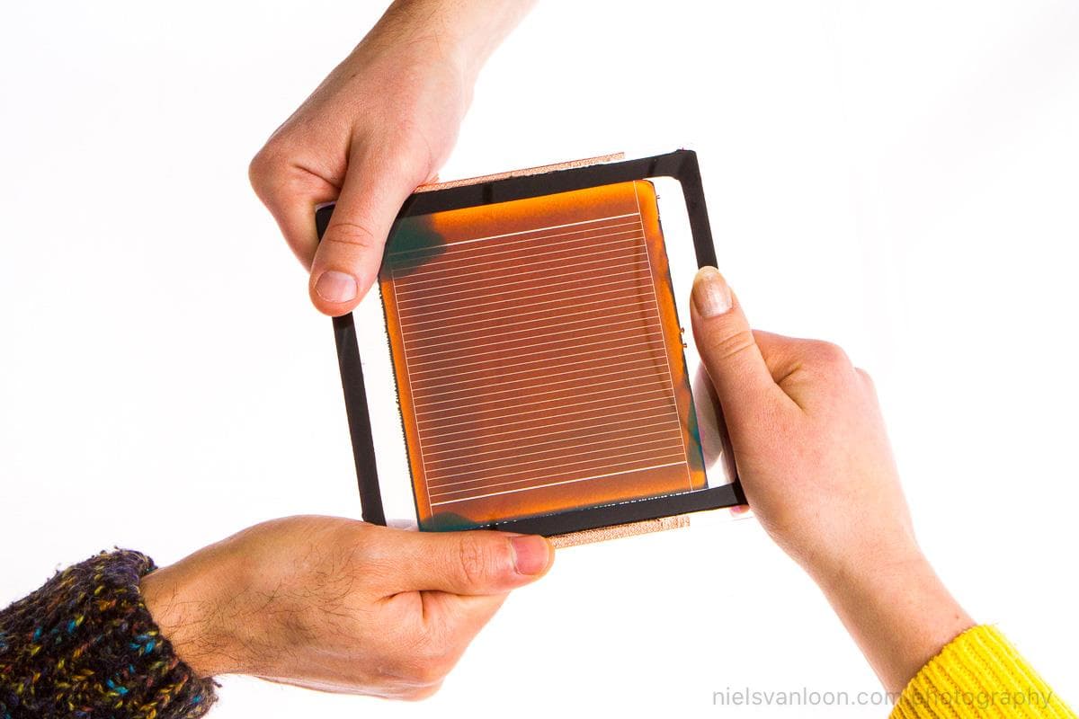
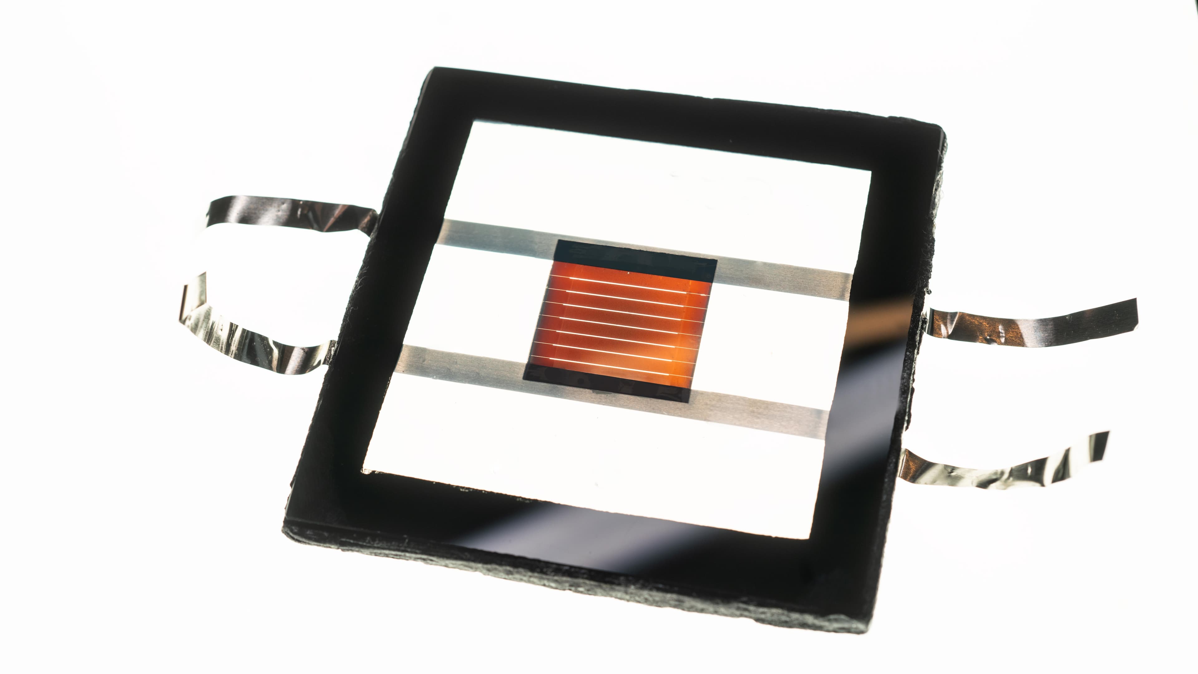
World’s first demonstration by Solliance partners TNO, imec/EnergyVille and TU/Eindhoven of encapsulated perovskite solar modules fabricated using industrial processes that withstand three established lifetime tests. (image © nielsvanloon.com/photography).
Throughout all of these activities – from materials, equipment and processes, over module and system integration all the way up to final implementation – the active involvement of industrial partners and the support from national and European public funding cannot be overestimated. At the very basis, the expertise of materials and equipment suppliers allowed rapid adaptation at the disruptive and exciting times when perovskites gained a reputation. Further down the road, glass manufacturers, building, and automotive companies' input and active involvement proved vital to develop suitable solutions for BIPV, VIPV, and other customized applications. And the combination of private and public funding allows for being involved at the forefront of innovation across the thin-film PV domain's full width. Looking back on the past decade's results and looking around at all the stakeholders and ingredients that are continuously growing in their maturity as a well-oiled ecosystem, one can only be enthusiastic and ambitious on where this can bring us in the decade to come. May it act as a warm welcome to everyone involved to maintain or increase their efforts or join in on the adventure for those who haven’t already.
Want to know more?
An overview of the most noteworthy thin-film PV achievements of the past 10 years in which imec was involved:
- 2011: imec, Solvay, Polyera reach OPV efficiency of 8.3% - Renewable Energy World
- 2014: 8.4% efficient fullerene-free organic solar cells exploiting long-range exciton energy transfer | Nature Communications
- 2016: Imec and its Solliance Partners Present First Semi-Transparent Perovskite Modules | imec (imec-int.com)
- 2017: Imec and Solliance’s perovskite PV modules achieve 12.4% | imec (imec-int.com)
- 2017: Press Release - Imec Reports Record Conversion Efficiency of 23.9 Percent on a 4cm2 Perovskite/Silicon Solar Module | imec (imec-int.com)
- 2017: imec magazine May 2017 - A city full of energy | imec (imec-int.com)
- 2018: Partner Related Press Release - The key to a sustainable building façade | imec (imec-int.com)
- 2018: Perovskite/CIGS tandem cell with Record Efficiency of 24.6 percent Paves the Way for Flexible Solar Cells and High-Efficiency Building-Integrated PV | imec (imec-int.com)
- 2020: Partner related - Scaled perovskite solar modules pass three critical stability tests. | imec (imec-int.com)
More details about the various actors:

Dr. Tom Aernouts received his M.Sc. in semiconductor physics in 1998, and a Ph.D. in Science in 2006, both from the KU Leuven, Belgium. He initiated the research on thin-film solar cells at imec in 1999. Working on the fundamental understanding of organic solar cells and developing bulk heterojunction solar cells and fully flexible modules until 2006, Tom has since led imec’s thin-film PV group, steering imec’s thin-film PV research activities. The group expanded its activities in 2014 with the work on hybrid, perovskite-based thin-film solar cells and in 2018, with the move to EnergyVille, extended the device size to 35x35cm². As of October 2021, Dr. Aernouts leads the merger of thin-film PV activities at imec and imo-imomec/EnergyVille, broadening the activity into CIGS, Kesterites and other novel material systems.

Dr. Jozef Poortmans is an imec Fellow and the Program Director of the Energy activities of imec since 2020. He received his degree in electronic engineering from the KU Leuven, Belgium, in 1985. He has been a part-time Professor at the KU Leuven since 2008, where he teaches on photovoltaics and materials in electrical engineering. In 2013, he also became a part-time Professor at University Hasselt where he teaches a course on analog electronics. In September 2016, he became the Coordinator of R&D-strategy at EnergyVille, an institutional partnership between imec, VITO, KU Leuven, and University Hasselt, which is focused on the themes of Smart Cities and Smart Grids.
Published on:
30 March 2021

