The road towards artificial diamond
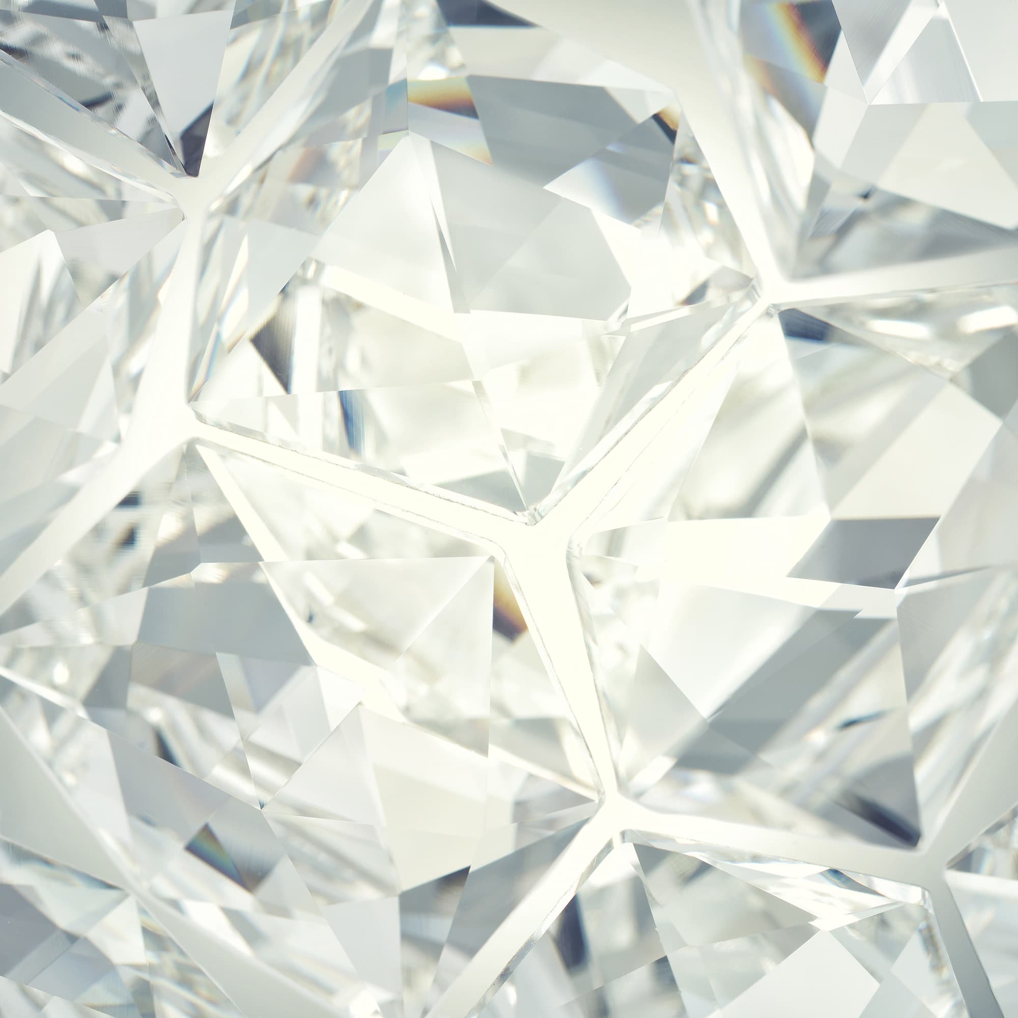
Diamond exhibits a unique combination of chemical, physical, thermal and mechanical properties, and this has triggered many scientists to replicate nature to fabricate diamonds. Original attempts to produce this material in a synthetic way date back from the 1950’s, and resulted in the first artificially produced diamond using high-pressure high-temperature (HPHT) synthesis. This HPHT diamond became a very important commercial material for the construction industry, which exploited the physical hardness of the HPHT diamond for cutting, sawing and drilling.
Later on, low-pressure synthesis methods for making artificial diamond outside its thermal stability domain were developed, aiming at potentially larger scales by using chemical vapor deposition (CVD). This allowed for the first time to grow diamond at low pressures of several tenths of mbar. Milos Nesladek from IMO-IMOMEC, an imec research group at University of Hasselt: “Basically, this CVD process involves a series of gas-phase and surface chemical reactions, using methane and hydrogen as the main gas constituents to form diamond material. This method of making artificial diamond has allowed to significantly improve on the purity of the material. Today, artificial diamond crystals can be thousand times and more purer than the best natural crystal.”
IMO-IMOMEC has a long track-record in depositing diamond on a variety of substrates, and in understanding the influence of the used deposition conditions, the crystal quality and materials properties.
“In general, the properties of artificial diamond largely depend on the subtle details of the manufacturing process”, adds Milos Nesladek. “Some artificial diamonds have properties such as hardness, thermal or electronic properties that are even superior to those of most naturally formed diamonds.”
A rising number of applications
Far beyond the construction industry, the evolution in synthetic production of diamond has enabled amazing applications – each exploiting a different characteristic of this ‘wonder’ material. A first example is the realization of dome-shaped CVD diamond membranes to replace conventional loudspeaker membranes in exclusive, high-end audio components. In this application, the high Young modulus of diamond – a measure for the material’s stiffness – allows the membrane to operate at high acoustic frequencies.
Milos Nesladek: “Other examples include diamond-based electrodes for electrochemical processing (such as purification or dissociation), which rely on the high electrical conductivity of heavily boron-doped diamond and on its low corrosivity. And, being optical transparent at a wide range of wavelengths, high-purity CVD diamond is being used in the ship industry as an optical window for infrared laser cutting of steel plates. Diamond is also a fantastic heat sink, and this has inspired scientists to use diamond heat sinks in combination with gallium-nitride (GaN), and make GaN-on-diamond-based power devices. The use of diamond significantly reduces semiconductor temperatures while keeping the power transistor’s performance, even at high operating frequencies.”
Quantum sensors for magnetic field detection
The ability to make 12C isotopically purified diamond has opened doors to exciting novel quantum technology applications. Key to these applications is the formation of a lattice point defect – the nitrogen-vacancy (NV) center – engineered in an ultrapure CVD-diamond crystal. This defect center has an electron spin state (expressing a magnetic moment), which behaves like a single spin qubit – the quantum-physical equivalent of the classical bit. A main striking property of this particular qubit over e.g. qubits made from superconducting materials or trapped ions and others, is its ability to operate at ambient conditions.

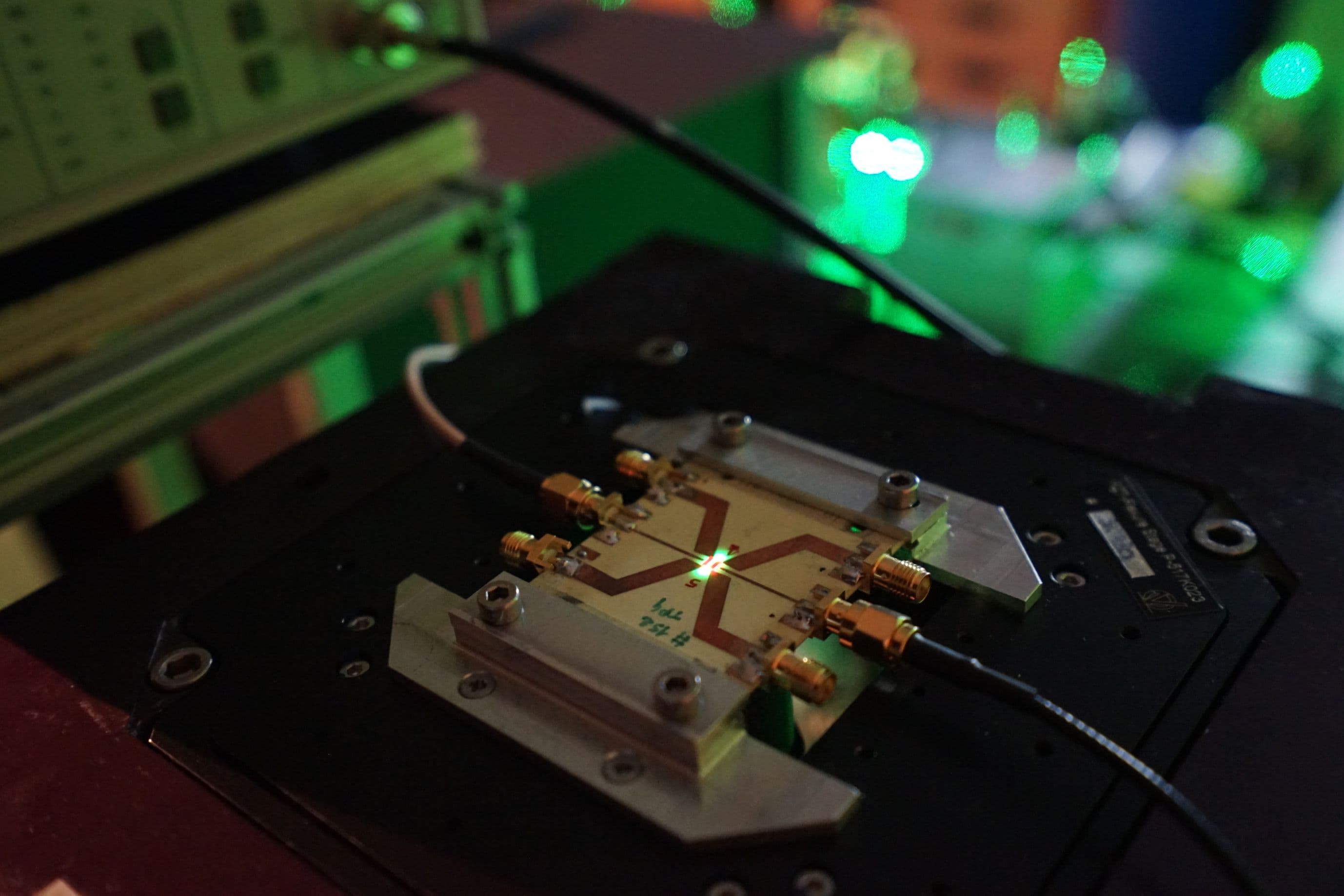
 Researchers at IMO-IMOMEC have created electrically readable qubits out of artificial diamond. The photographs show a diamond quantum device mounted on a microwave (MW) board for qubit addressing under pulsed green laser illumination providing spin initialization.
Milos Nesladek and his colleagues at IMO-IMOMEC use the NV centers in diamond mainly to develop quantum sensors for magnetic field detection. “In these applications, the spin related to the NV center undergoes rotations during operation”, explains Milos Nesladek. “If there is interaction with an external magnetic field, this translates into a phase delay that can be measured using quantum protocols. Based on this phase delay, the external magnetic field can be determined much more accurately than with any existing device.”
So far, readout of the spin state of these solid-state qubits at room temperature could only be performed optically, using bulky optical setups. Recently, researchers at IMO-IMOMEC have discovered a way to address single NV centers electrically, as described in Science Magazine (February 2019). It is hoped that this finding will bring a major step towards device miniaturization and integration with semiconductor platforms, and that it will boost the fabrication of compact magnetometers and other applications.
From battery monitoring to medical diagnostics
Diamond quantum sensors for electromagnetic field detection can potentially become the first quantum devices on the market. A promising industrial application is the very accurate monitoring of the battery economy in e.g. electric cars. One common way to measure a battery’s state-of-charge is Coulomb counting – based on measuring the in- and out-flowing current. But traditional coil-based methods are not able to measure these currents very accurately. This challenge can be overcome by using the highly sensitive diamond quantum sensors. With this precise monitoring, the driving range of the electric car can be predicted much more accurately. And this has raised the interest of electric car producers.
Quantum sensors are a more sensitive alternative to giant-magnetoresistance (GMR) devices, used in satellites for navigation. Milos Nesladek: “The sensitivity of quantum sensors can outperform GMRs with roughly a factor of thousand, while vector operation allows precise navigation in the earth magnetic field. However, to compete with today’s (cheap) GMR devices, researchers need to increase the cost-effectiveness of the diamond quantum sensors.”
Finally, engineering of solid-state qubits in ultrapure diamond can be used for realizing nuclear magnetic resonance (NMR) devices on a chip. Giving access to the chemical analysis of molecules in sub-nanoscopic volumes, these NMR lab-on-chip devices can be deployed for e.g. drug development or medical diagnostics. For some applications, they can replace the bulky, expensive and less sensitive NMR setups that exist today. “The technologies behind these quantum devices are currently being explored in a number of European projects (i.e., ASTERIQS, Q-Magine and NanoSpin, part of the European Quantum Flagship) involving collaboration from IMO-IMOMEC,” states Milos Nesladek. “Meanwhile, first start-ups in this field have also emerged. It is expected that first commercial NMR-on-chip devices will be on the market within five years from now.”
In the race for quantum computing?
There are currently numerous candidate platforms for quantum computers, including (but not limited to) trapped ions, superconducting qubits, integrated photonics, dopants in silicon and electrical quantum dots, each with very particular advantages. All of these operate at cryogenic temperatures.
‘The race’ for the most scalable and engineering system is however open and solid state qubits such as diamond or SiC would have great advantages because they can work at ambient.
However, today, a few challenges lay ahead for the ‘diamond’ qubit platform. More particular, quantum processors make use of several characteristics, including the quantum superposition (i.e., qubits can with a certain probability be zero and with a certain probability be one) and entanglement (i.e., qubits can talk with each other and act concertedly). This allows them to efficiently tackle problems that are inaccessible to current-day computers.
Realizing a scalable superposition and entanglement in diamond is the bottleneck of the problem. Milos Nesladek: “First, the NV centers need to be put at very close distance (within 50nm distance) to allow efficient coupling between the centers. This requires high-resolution lithography techniques. Second, single shot spin readout at ambient is a critical capability for establishing the NV center as a viable qubit candidate. But today, the probability with which we can read the spin state of the NV center at room temperature is only 30%. To increase this probability, the readout operation should be repeated many times. Nevertheless, at moderately low temperatures, i.e. 5 – 10 Kelvin, this probability can reach close to 100%. So we need techniques that can enhance the probability of the spin-state readout at room temperature. Today, we are working on both issues, and I’m optimistic that we can solve them in the near future. The race for what is the best quantum system is still open, and I think that NV centers in diamond may have a pretty good chance...”

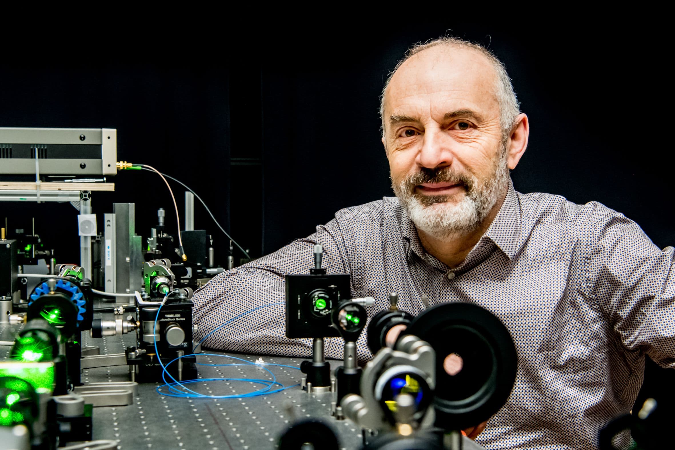
Milos Nesladek and his team at IMO-IMOMEC, including Emilie Bourgeois (who is specialized in optical transitions in semiconducting materials), Michal Gulka (who works on spin readout protocols) and Tanmoy Chakraborty (previous group member). Several PhD and master students are involved in this work, namely Jaroslav Hruby, Jelle Vodnik and Jeroen Prooth. The team collaborates with the group of Iuliana Radu from imec, who uses silicon as a base for quantum computer technology.
This project has received funding from the European Union’s Horizon 2020 research and innovation programme under grant agreement No 820394 (ASTERIQS – Quantum Flagship project), DIAQUANT SBO project S004018N from FWO and Q-Magine, an ERA-NET project in the framework of the Quantum Flagship.
Want to know more?
The paper ‘Photoelectrical imaging and coherent spin-state readout of single nitrogen-vacancy centers in diamond’, by Petr Siyushev et al. – recently published in Science Magazine (February 2019) – can be requested via this link.

Prof. Milos Nesladek, PhD, obtained his MSc. degree from the Faculty of Mathematics and Physics, Charles University in Prague, and the PhD degree from the Czech Academic Sciences, in collaboration with KU Leuven in the field of electronic transport in semiconductors. He is a professor of physics at the University of Hasselt and a member of staff at IMO-IMOMEC, an imec research group at University of Hasselt. He is one of the pioneering scientists in the field of growth of CVD diamond crystals in all forms, being in that field for the last 30 years. Prof. Nesladek’s research topic deals with photoconduction in condense matter systems with emphasis on wide-bandgap semiconductors. An example of this research is the development of photoelectrically read solid state Q-bits in diamond based on paramagnetic spin centers. Prof. Nesladek has participated in a large number of EU projects ranging from basic physics to industrial development projects which, some of them, he has coordinated. Prof. Nesladek is member of several conference boards and he is the Belgian representative to the Quantum Community Network (QCN) of the Quantum Flagship. Prof. Nesladek published over 300 scientific papers and contributed to several books. He is associated editor of Diamond Related Materials.
Published on:
7 May 2019


