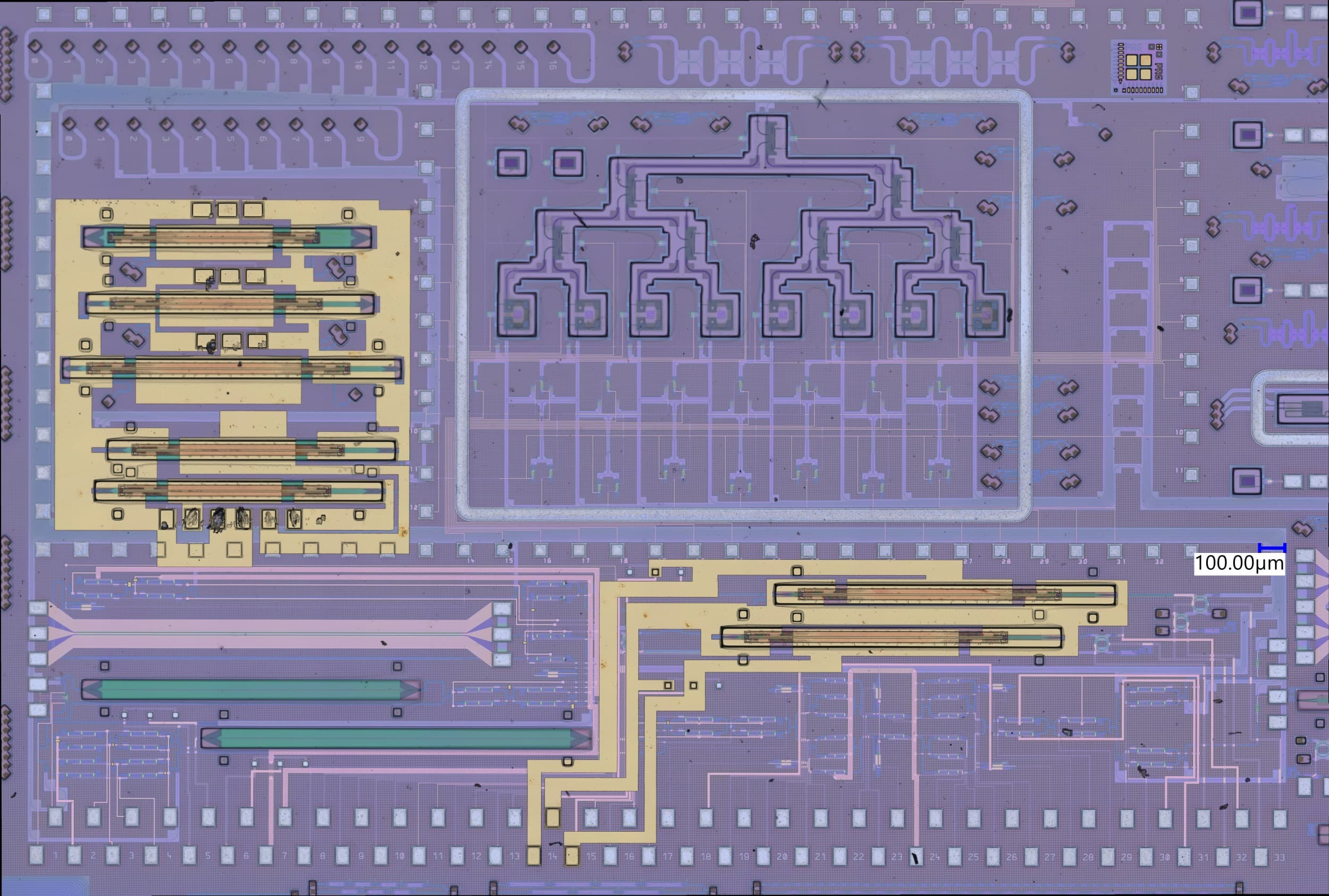
Today, the amount of data stored in the world is a thousand billion gigabyte and this will keep on increasing exponentially e.g. with the internet of things. The capacity of data centers needs to increase if we want to keep using all our current and future Internet applications. Silicon photonics plays an important role in doing just that. It promises fast data traffic, with compact components that consume little energy. And imec is investing heavily in this technology. In 2016, our researchers demonstrated a unique germanium-silicon modulator with a 56Gb/s bandwidth. This modulator enables compact, efficient optical links to be made for server-to-server communication in data centers. Recently, this modulator was developed further and used into a 16-channel 896Gb/s prototype transceiver, integrated in a photonic chip measuring just 1.5mm². It has also been demonstrated in conjunction with Ghent University that the modulation speed per channel can be increased further to 100Gb/s. These results were recently presented at the prestigious OFC conference in Los Angeles, the leading forum for groundbreaking research into telecoms and datacoms.
Making the cloud bigger
Every day we produce massive quantities of data. You only have to think of e-mails, text messages, pictures and videos posted on social media, data from your fitness watch, etc. to see why. And the quantity of data processed by companies such as Google, Facebook, Microsoft and Amazon is growing exponentially. Then there’s the Internet of Things where all kinds of things will be equipped with sensors taking measurements and communicating with one another. All of which means even more data.
All of this data is stored and processed in the cloud – i.e. in a data center. Data centers are where thousands of servers sit quietly in racks, all communicating with one another via a complex network of optical fibers. To meet growing demand, this network also has to be upscaled exponentially. The roadmap for this server-to-server communication is extremely ambitious: since 2016, the most advanced cloud data centers have installed optical links and transceivers with a capacity of 100Gb/s; By 2019 an upgrade to 400Gb/s is expected and by 2022, this will be upscaled further to 1.6 Tb/s.
Cloud data centers are also very large facilities and the optical links they contain need to have a range of at least 500 meters. The optical links for cloud data centers also need to be manufactured in much greater volume and at substantially lower costs than the traditional telecoms solutions.
The complex network of optical fiber connections in a cloud data center (Facebook)
Silicon photonics
Silicon photonics is an interesting technology for integrating the essential building blocks required for an optical link in a single chip. The big benefit of this technology is that the optical components can be produced using the same advanced devices with which microchips are also made. This makes silicon photonics components relatively cheap. Better still, they make a high integration density possible, while consuming less energy and guaranteeing a high yield.
Imec has developed a platform for silicon photonics for high-speed optical links for data, telecom and sensing applications. voor hogesnelheid optische links voor data- telecom- en sensor-toepassingen.. It uses 200mm and 300mm SOI wafers (silicon-on-isolator wafers) as its substrate. The manufacturing process is based on a modified 130nm CMOS flow, expanded by 193nm lithography to produce the waveguides, using germanium for the photodetectors. An additional oxide/poly-silicon stack provides greater freedom when designing the optical components. This stack is used to integrate passive components such as grating couplers for optical fibers, waveguides and multiplexer filters. With the integration platform, both passive and active components (such as opto-electronic modulators, heaters and germanium-on-silicon photodetectors) can be integrated. Electronic circuits (such as drivers and transimpedance amplifiers (or TIAs)) can be made on a separate chip and assembled with the silicon-photonics circuit using flip-chip techniques (packaged into one system). In these circuits, the driver converts a standard CMOS-bit signal into an electrical current that is compatible with the optical chip, while the TIA amplifies the photo-electric current into a standard CMOS-bit signal.
Imec’s 50Gb/s silicon photonics platform and devices
Very compact low-power transceiver with a 10x higher bandwidth than current transceivers
Wavelength division multiplexing (WDM) and space division multiplexing (SDM) are two ways of increasing the bandwidth of optical links. With WDM, the signals are encoded onto different carrier wavelengths and all of these wavelengths are sent through the same optical fiber. This reduces the cost, especially over long distances. But there are also disadvantages: optical insertion losses and wavelength filters that are very temperature-sensitive, resulting in the power efficiency being negatively affected.
For this reason, SDM is a good alternative, certainly for short distances. Indeed, in this case, the cost of the optical fiber is not of overriding importance. With SDM, a fiber is used with various cores through which light from one specific wavelength is sent in parallel. Today, four parallel single-mode fibers are used for 100Gb/s optical links.
At OFC2017, the leading optical communication conference, imec exhibited a unique building block from its silicon photonics platform, integrated into a very compact SDM transceiver. The total bandwidth of this transceiver is 896Gb/s, while the transceivers in current data centers are only capable of 100Gb/s. This result indicates that photonics will play an important role in making it possible to adhere to the ambitious roadmap for data centers.
The transceiver consists of a series of 16 GeSi electro-absorption modulators (EAMs) on the transmitter side and 16 GeSi photodetectors on the receiving side, all integrated on to a single chip. All modulators have a bandwidth of 56Gb/s. The photodetectors are based on the same structure as the modulators, but work with a different bias voltage. The modulators and photodetectors are located very close to one another, at a distance of 100 micrometers, meaning that the transceiver is very compact. The waveguides are also compact and tightly integrated, as are the power splitters and fiber grating couplers of the optical fibers. Because both the transmitting and receiving sections are made from the same GeSi material, production is very efficient and affordable.
Top: Scheme of compact 896Gb/s SDM transceiver (<1.5mm²) with an array of 16x56Gb/s GeSi NRZ-OOK modulators (transmitter) and photodetectors (receiver). Below: To test the quality of this transceiver, the eye diagrams of all 16 modulators and photodetectors were examined. They are all nice, open eye diagrams, which show that the signal can be sent and received without any bit errors.
Single-channel 100Gb/s optical link with silicon photonics modulator
Working in conjunction with researchers from UGent, imec also demonstrated the first real-time single-channel 100Gb/s non-return-to-zero on-off-keying optical link in silicon photonics. The same ultra-compact GeSi modulator was used for this. It was combined with a transceiver chip designed by UGent in SiGe BiCMOS technology. The signal transfer via this optical link was tested over a standard single-mode optical fiber (SSMF) 500 meters long and a dispersion-shifted optical fiber (DSF) 2 km in length. This signal transfer was successful without any complex digital signal processing (DSP) being required. This result shows that silicon photonics is the right technology for producing compact, low-power transceivers with scalable capacity for future server-to-server connections.
Real-time 100Gb/s NRZ-OOK 1-channel optical link with the GeSi modulator.
Interested in silicon photonics components?
The GeSi modulator used in the two demonstrators above is available for companies and research groups, as are other components from imec’s silicon photonics platform. This can be done via the imec-ePIXfab SiPhotonics:iSiPP50G service, which is part of the Europractice silicon photonics multi-project wafer (MPW) service.
Want to know more?
You can retrieve the technical papers about the results mentioned above via imecmagazine@imec.be. The titles of the papers are ‘Ultra-dense 16x56Gb/s NRZ GeSi EAM-PD arrays coupled to multicore fiber for short-reach 896Gb/s optical links’ and ‘First real-time 100Gb/s NRZ OOK transmission over 2 km with a silicon photonic electro absorption modulator.’
Want to find out more about the silicon photonics multi-project wafer service? If so, please contact Phillip.Christie@imec.be. Or if you would like more general information about the silicon photonics prototyping service, then please contact Kenneth.Francken@imec.be
Published on:
5 May 2017


