Stacking chips on top of each other is a well-known approach to make more compact and powerful systems. Just think of more memory for your cell phone or a more powerful graphics processor for your laptop. Until now, it was impossible to probe the large arrays of fine-pitch micro-bumps on advanced chips before stacking. This had a negative effect on the compound yield (because of including faulty dies in the stack). Imec, together with FormFactor (formerly Cascade Microtech), has developed a unique fully-automatic system to probe these micro-bump arrays.
Stacking chips in 3D packages is seen as the way forward to building more powerful systems. It compensates for the laws of physics that threaten to push chip makers off the path of Moore’s Law. For example, you can stack different memory chips on top of each other to make compact and high-capacity memory stacks. Also, it allows to combine different types of chips, e.g., a logic and memory chip, or a FinFET-based logic chip and a planar CMOS logic chip. You could say that 3D unites different technologies and in this way is an important enabler for future Internet of Things products where miniaturized systems based on different technologies will make their mark.
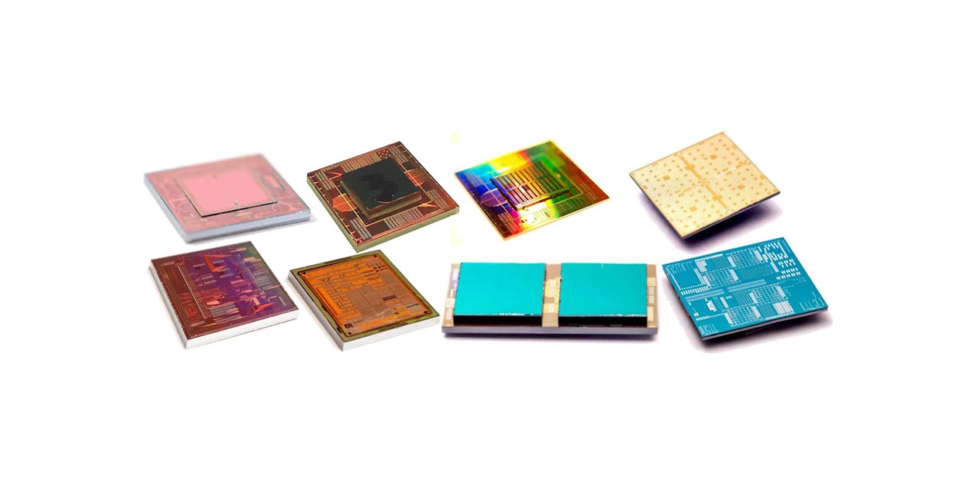
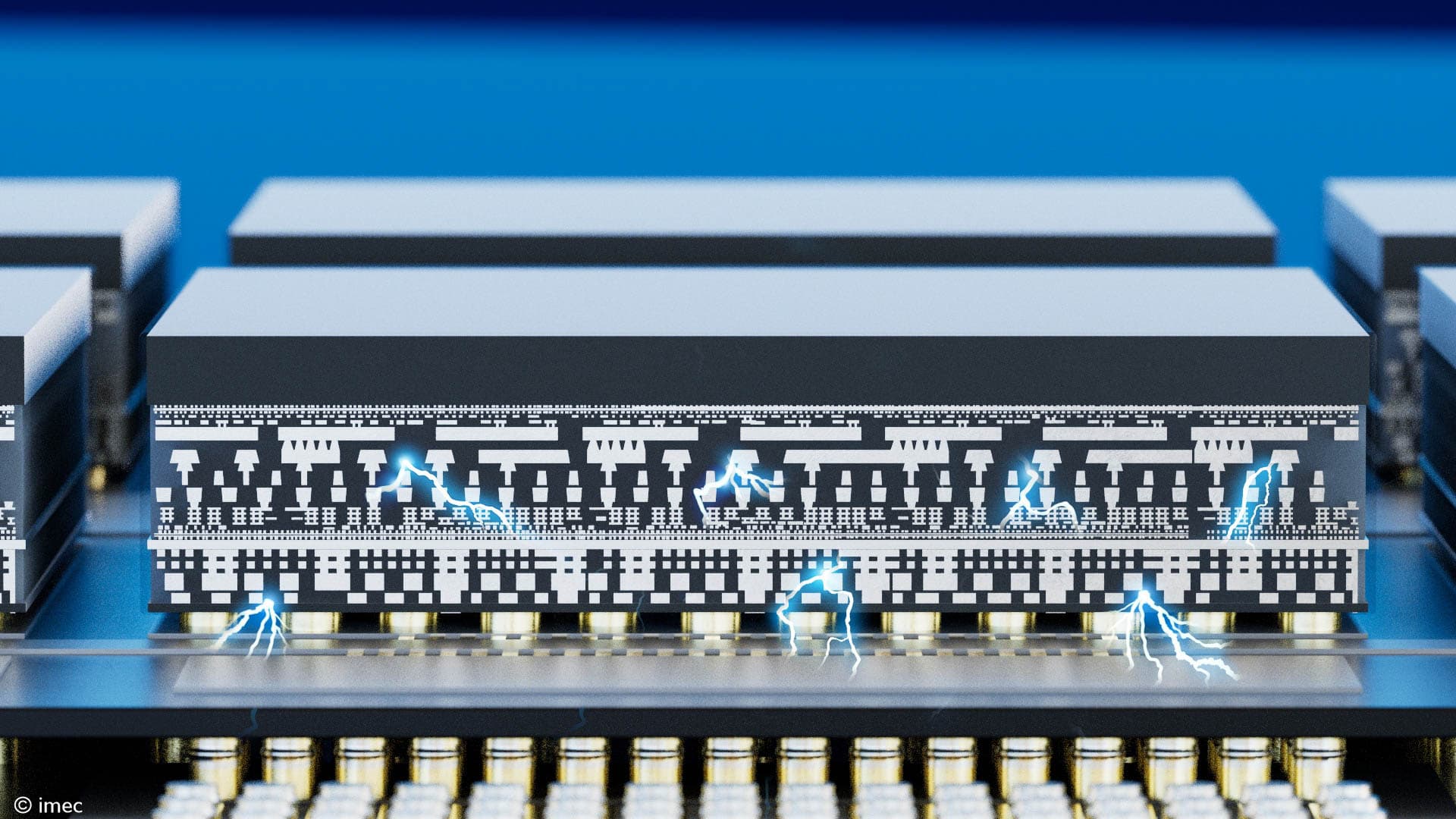
Examples of 3D stacked test chips at imec.
As an emerging technology, 3D stacking still has many open options and technical challenges. One of these is the probing of chips before being stacked, and hence ensuring a good yield of the 3D chip stacks. The inter-chip connections are made by large arrays of fine-pitch micro-bumps and it was considered ‘impossible’ to probe these bumps because they are so numerous (≥ 1000) and so close to each other (≤40 micrometer). The current solution is to add dedicated probe pads to the chips, but this requires extra space and design effort and leaves the micro-bumps untested.
In 2010, Cascade Microtech (now FormFactor) and imec started their collaboration to tackle the fine-pitch micro-bump probing issue. This has resulted in the development of a full-automatic test system for characterizing advanced micro-bump probe cards. The system is based on the Cascade CM300 probe station from FormFactor, and National Instruments’ PXI test instrumentation. Also, software for automatic test generation and data analysis and visualization was developed. The test system was installed in imec’s cleanroom to perform experiments.
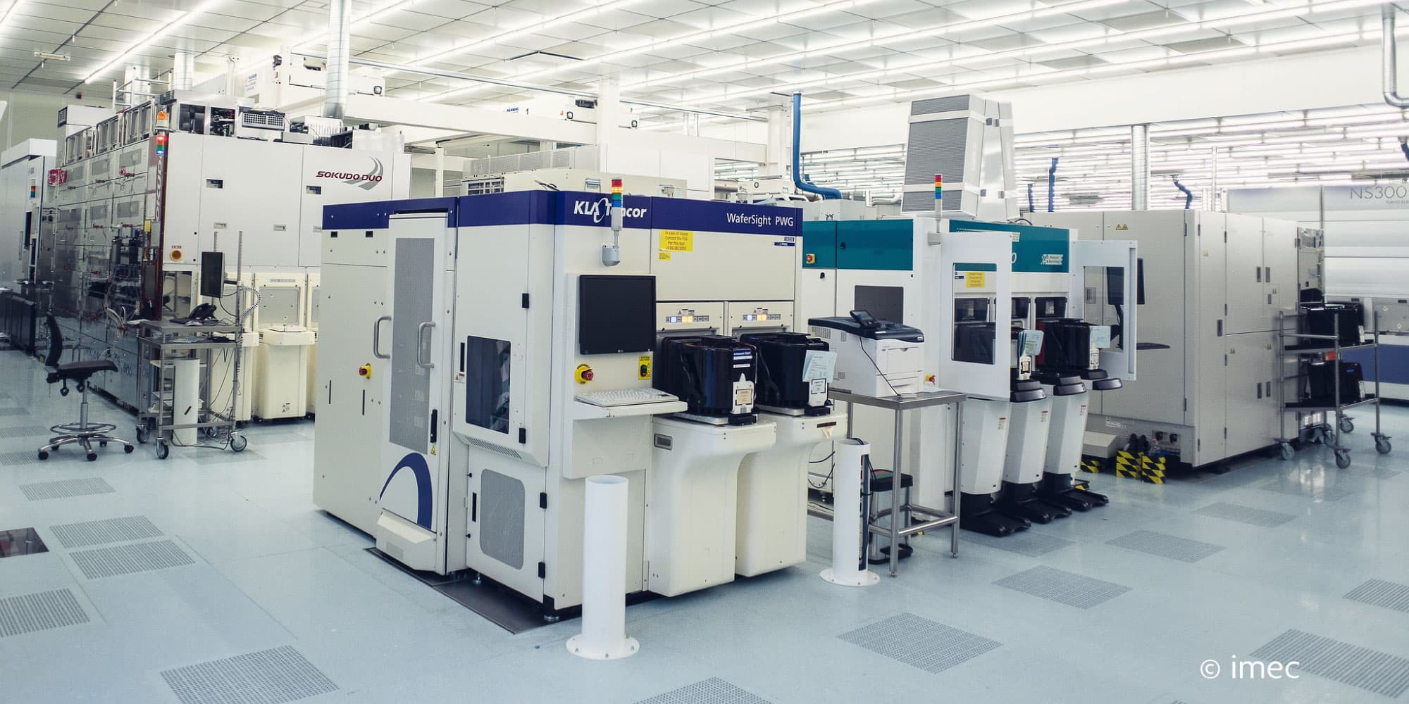
Full-automatic test system for direct micro-bump probing installed at imec’s cleanroom.
Probe card and core as used in the new test system. This was provided by the leading probe-card supplier FormFactor. The probe core includes thin-film technology with MEMS-type probe tips.
The system was successfully used for micro-bump arrays as defined by the JEDEC standardization organization for Wide-I/O single data rate DRAM memories. Both JEDEC WIO1 and WIO2 micro-bump arrays were successfully probed, with a minimum pitch of 40 micrometer and a maximum array size of 1200 (= WIO1) and 1752 (= WIO2).‘Successful’ in this context means that the test system has a sufficient number of channels for the number of micro-bumps; all the probe tips land on the micro-bumps and make good electrical contact, without damaging the micro-bumps; and – last but not least – the approach is economically feasible.
All tests were performed on 300mm test wafers, designed and manufactured at imec and containing micro-bumps with various metallurgies, pitches, diameters, and array sizes. The system is now being used routinely to test imec’s micro-bumped wafers. While today’s advanced micro-bump processes are at 40 micrometer pitch, this is, as everything in the semiconductor world, subject to miniaturization. Hence, imec and FormFactor have already started to probe micro-bump arrays at 20 micrometer pitch.
Want to know more?
Read a more detailed article on the website of National Instruments. This paper was selected as finalist for the 2017 NI Engineering Impact Award in the category ‘Electronics and Semiconductors’.
Published on:
5 June 2017

