Best of 2016 / Edition September 2016
Osceola county is a fast-growing innovation hotspot situated in the lush heart of Florida, some 30 kilometers south of Orlando. Here imec has found the support and contacts to set up a new hub for its USA activities, which was officially established beginning of the summer, on July 8. Imec Florida’s activities will be focused around the design of innovative solutions using photonics and high-speed electronics. It will bring imec’s expertise closer to USA-based semiconductor and system companies, universities, and research institutes. Heading the new center as general manager will be Bert Gyselinckx, previously head of imec The Netherlands. Bert gives us a short tour of the new center.
An opportunity close to the partners
It has always been imec’s aim to keep close contacts with its partners. Even in today’s hyperglobalized markets, being embedded locally often proves a great asset.
That is why in the past we have set up local R&D hubs e.g. in Taiwan and China. And why, for some time already, we were looking to set up a research center in the USA, one of our strongest markets and the home turf of many of our partners. Such a local center would not only bring us closer to some of those partners, but it would also give them additional possibilities to leverage imec’s expertise, e.g. in USA federal projects.
Therefore, when Osceola County in Florida offered us a chance to establish a design center, we were immediately interested to investigate the opportunity.
Osceola County is fast becoming a new innovation hotspot, thanks to the efforts of the Florida and Osceola authorities and the proximity of UCF (University of Central Florida). Equally important is the establishment of ICAMR (International Consortium for Advanced Manufacturing and Research), which is in the process of setting up a state-of-the-art production specialized in IoT sensor manufacturing.
Working on the details of the collaboration, we’ve experienced an enormous drive by all partners to make this a success, with clear added value for everyone involved. We therefore are sure that imec Florida will soon thrive and deliver results that will benefit the regional high-tech community but also our USA and worldwide partners.
Focus on photonics and high-speed electronics
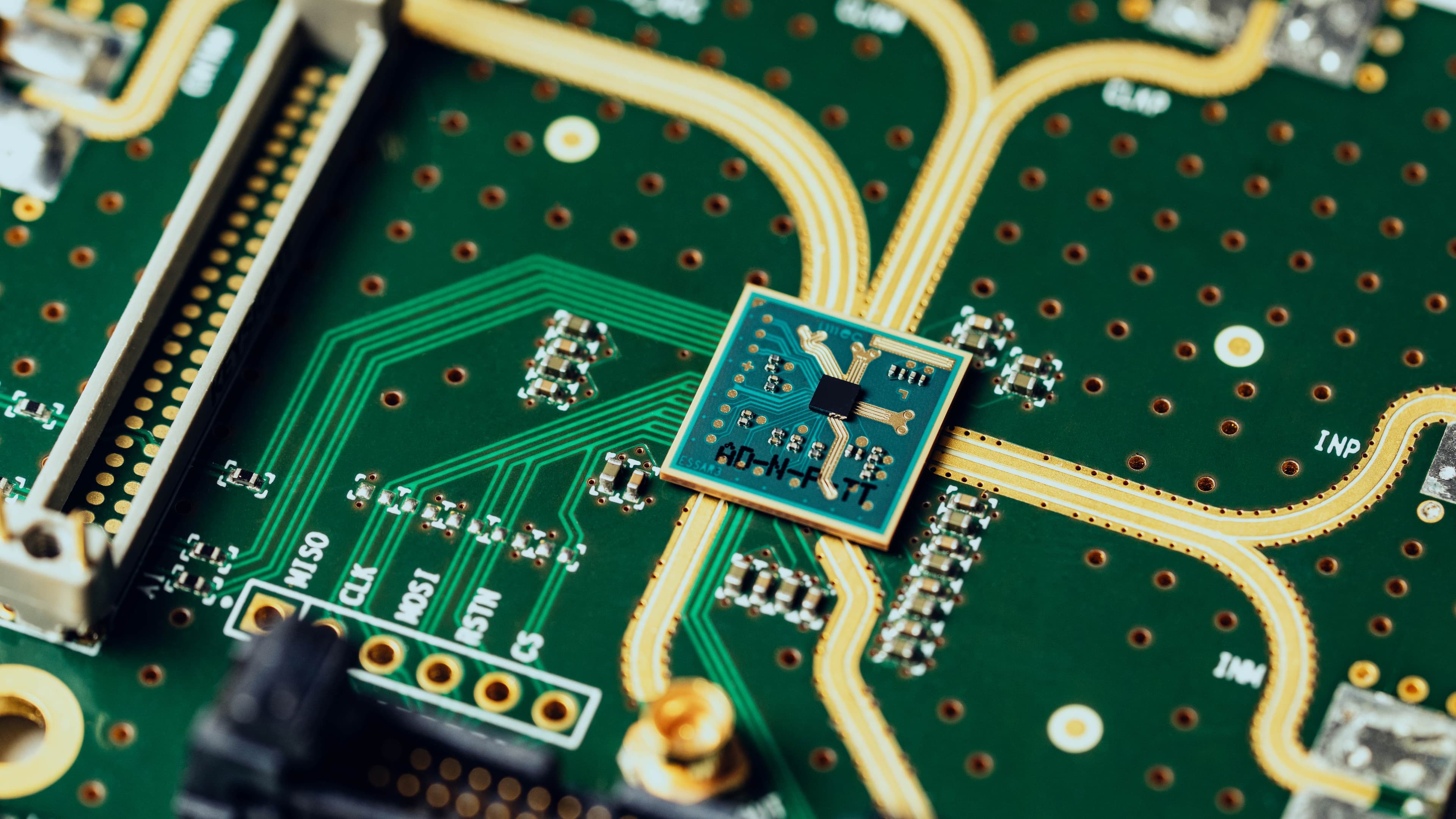
As an initial focus, imec Florida will concentrate on high-speed electronics (e.g. mm-wave imaging), photonics (e.g. LiDAR), and specialized imagers (e.g. IR and THz imagers).
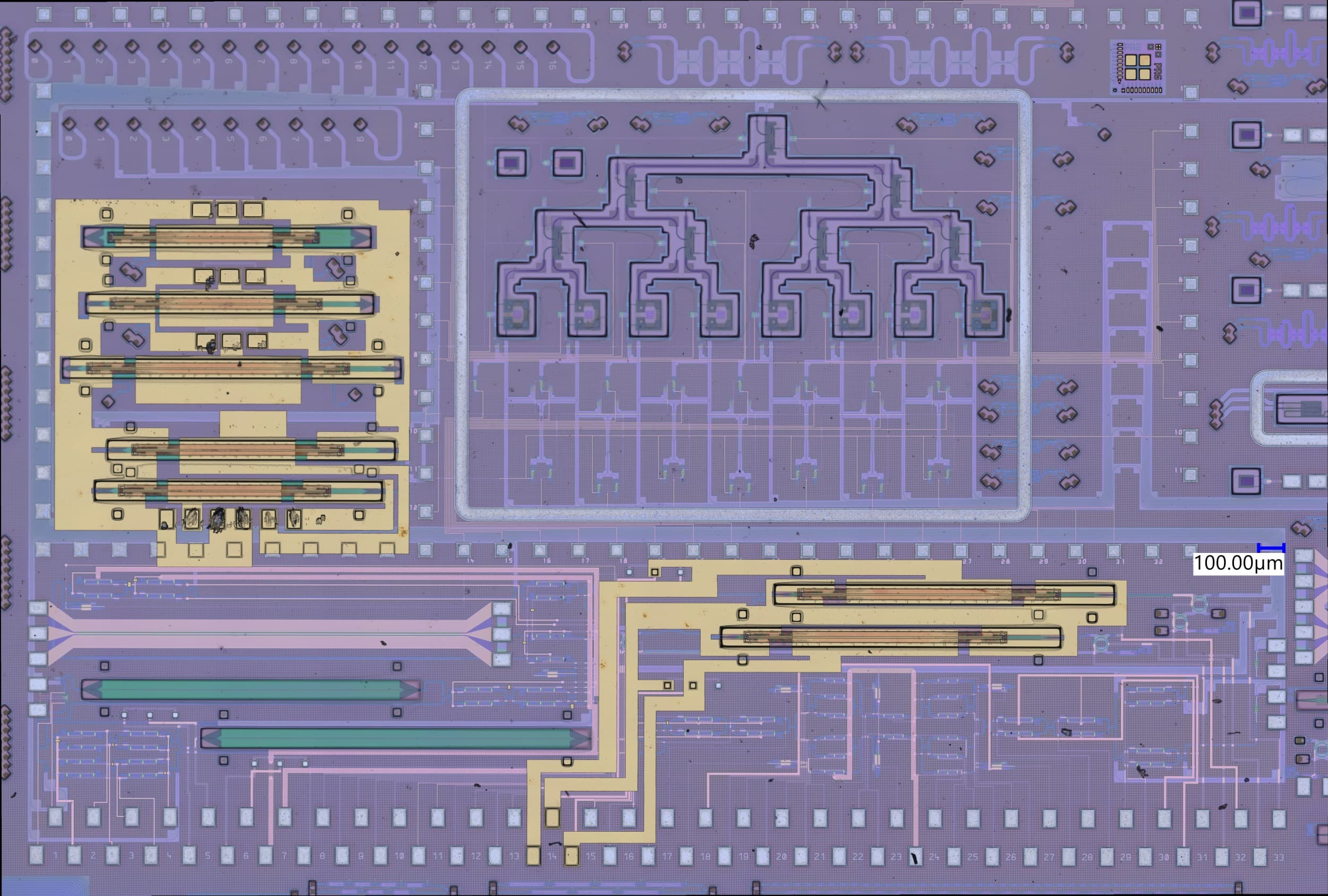
Long the exclusive subjects of university labs, photonics and high-speed electronics are two technologies that are gearing up for prime time. Think of the need to integrate photonics for high-speed interconnects between cores in multicore, heterogeneous, or 3D chip designs. And there are also countless new applications opening up for photonic sensoring, e.g. in healthcare, machine vision, autonomous driving, artificial intelligence and the IoT.
Imec has been a pioneer in the industrialization of these advanced technologies. We have been developing them in our Leuven headquarters with remarkable success. They are an excellent fit for the new center because they have the potential to be disruptive in a number of domains that are strategic for the USA market, such as healthcare, aerospace, security, and transportation. And as an additional asset to the new center, our partner university (UCF) also brings an extended experience in photonics to the table.
One of the headline applications that will be developed at imec Florida is a micro-sized, all silicon, low-cost LiDAR technology. A LiDAR application forms an image of the environment by shining it with a laser and capturing the reflected light to compute distances. LiDAR applications have been in use for decades, but they have never been made in miniaturized, silicon-only packages. Doing so will open up LiDAR technology for all kinds of new applications, foremost autonomous driving but also intelligent machine vision and robotics, monitoring of near-surface soil content, monitoring of vegetation health, wetland inspection, fisheries monitoring, coastal erosion mapping, minefield mapping, and much more.
Short and mid-term plans
Starting today, we’ll be looking to attract top talent for our new center. The short-term goal is to have ten experts up to speed by the year’s end, and gradually grow from there to a headcount of around 100 specialists.
One of the activities of imec Florida will be to offer a much-needed suite of services for local initiatives that want to develop and manufacture innovative electronics but cannot do so because they lack the expertise and access to the semiconductor industry. Take e.g. SMEs or research centers that are planning and developing a high-value application, e.g. a sensor to monitor industrial machinery. As part of their strategy to access the market fast, they will want to fabricate prototypes and a low-volume first run of their product. However, in most such cases, the volumes they are going to need are too low to get access to the highest quality services of large foundries. This is where imec can make a difference and provide a solution.
It is our experience that some SMEs and R&D groups favor the availability of a local, approachable design center and an associated fab. So as an added asset, imec Florida is close to the ICAMR fab facilities, with which we have a partnership. ICAMR is a consortium initiative with the goal to develop advanced lab/fab and universal technology platforms for advanced sensors and other future high-tech products (emitters, modulators, energy and communications devices/systems). The ICAMR fab will specialize in technologies such as the ones designed at imec Florida, and will be one of the fabrication options for SMEs and R&D groups that have their designs made by imec.
For companies in the USA market want to take their applications and sensors to the next level, we will complement the services of imec Florida with those of IC-Link. IC-Link is the industrial arm of imec and provides low-cost access to worldwide advanced foundry services.
And last, true to our spirit as a global R&D center, imec’s global partners will also be able to profit from imec’s advanced knowledge and experience in innovative photonics and high-speed electronics IC design.
Published on:
19 September 2016


