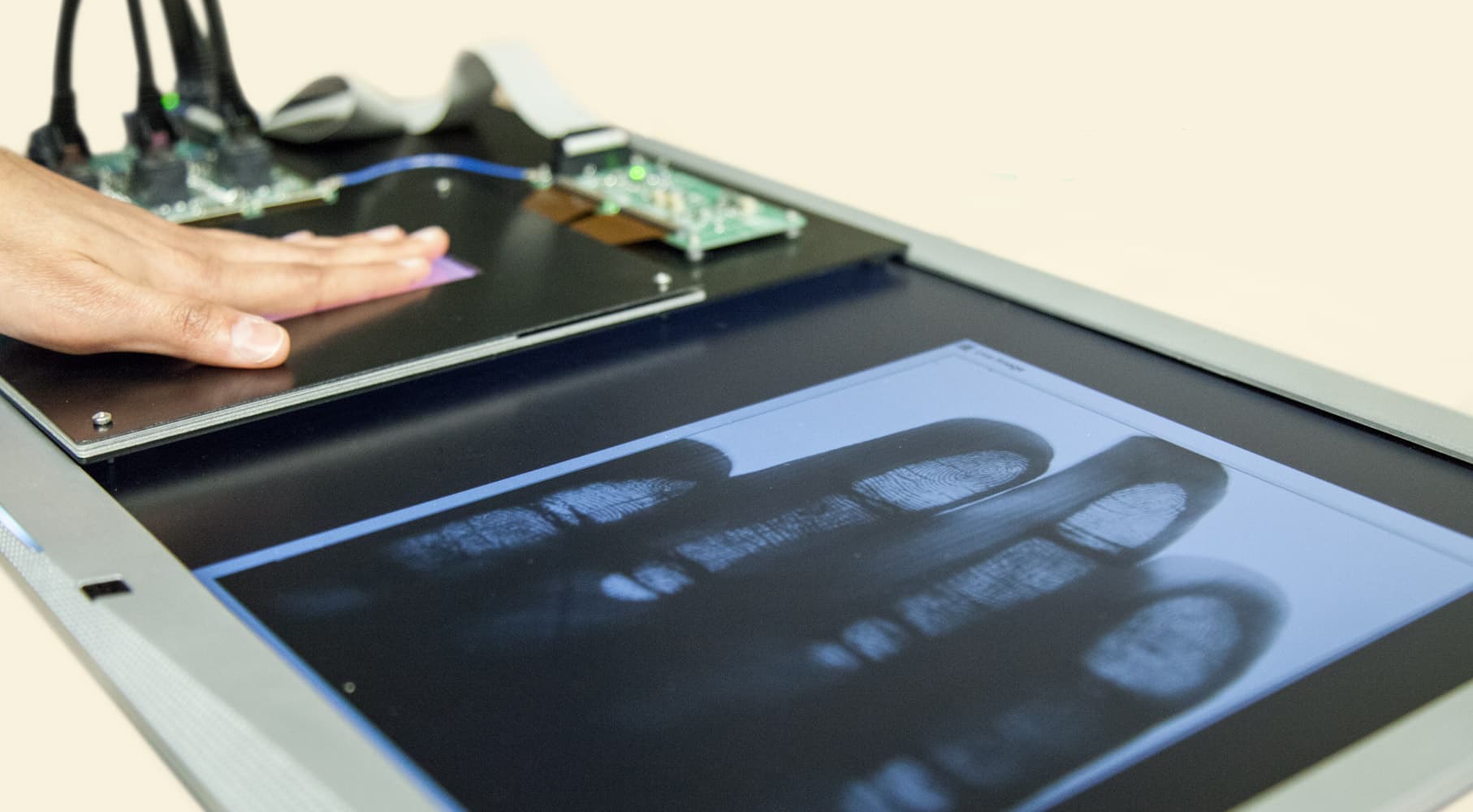
Researchers from Holst Centre, an open innovation initiative of imec and TNO, have demonstrated a new class of flexible, large-area sensor technology for detecting finger- and palmprints. At less than 0.2 mm thick and with no bulky prisms or moving parts, the new sensors can be embedded into objects such as mobile phones and door handles to create “invisible” yet secure access control systems that can tell if the print is from a living person rather than a phantom or counterfeit.
The technology, which paves the way to low-cost sensors for large-area finger- and palmprint scanners, will be on show at the Innovation Zone at the Society for Information Display (SID) Display Week 2018 in Los Angeles, USA from 22 to 24 May, and the Imec Technology Forum (ITF) in Antwerp, Belgium from 23 to 24 May. Two demonstrators will showcase the technologies potential for high resolution and large active areas. Measuring 6 x 8 cm, a 200-ppi demonstrator is large enough for 4-finger scanners that are currently used by border control authorities and delivers sufficient image quality for basic identification applications. Meanwhile, a slightly smaller 500-ppi demonstrator offer even higher image quality, compatible with FBI standards and enough for law enforcement agencies to visualize minutia and pores for more robust identification.
As with Holst Centre’s earlier flexible X-ray detectors, the fingerprint sensors combine an organic photodiode frontplane, an oxide thin-film transistor (TFT) backplane (originally developed for flexible displays), and a thin-film barrier for protection against the environment. All three technological elements have been or are being transferred to industry for scale-up and commercialization. The sensors read the finger- or palm print by detecting visible light (400 to 700 nm) reflected from the surface of the skin. However, they can also detect light that penetrates someway into the skin before being reflected. This allows them to sense a heartbeat from changes in the capillaries within the hand, and thus verify that the print comes from a live person.
Moreover, by using different photodiode materials, the sensors’ capabilities can be extended to other wavelengths such as near infrared (NIR). This could enable new identification verification modes based on for example the pattern of veins in a hand, which is believed to be even more specific to an individual than a fingerprint. NIR sensors could also be used in other applications, such as blood oxygenation monitoring, or for night vision and 3D facial recognition.
“The flexible fingerprint sensor demonstrator shows the versatility and maturity of the flexible electronics technologies that Holst Centre is developing. With the underlying technology already in use in the flat-panel industry, there is a fast route to manufacturing and we are looking for industrial partners to take that step,” says Hylke Akkerman, Program Manager at Holst Centre.

About Holst Centre
Holst Centre is an independent R&D center that develops technologies for wireless autonomous sensor technologies and flexible electronics, in an open innovation setting and in dedicated research trajectories. A key feature of Holst Centre is its partnership model with industry and academia based around roadmaps and programs. It is this kind of cross-fertilization that enables Holst Centre to tune its scientific strategy to industrial needs.
Holst Centre's fundamentals are to contribute to answering global societal challenges in healthcare, lifestyle, sustainability and the Internet of Things. This is visible through the motivation of its researchers, its different collaboration models and the choice of its research topics.
Holst Centre was set up in 2005 by imec (Flanders, Belgium) and TNO (The Netherlands) and is supported by local, regional and national governments. Located on High Tech Campus Eindhoven, Holst Centre benefits from, and contributes to, the state-of-the-art on-site facilities. Holst Centre has over 200 employees from some 28 nations and a commitment from more than 50 industrial partners. For more information visit www.holstcentre.com.
About imec
Imec is the world-leading research and innovation hub in nanoelectronics and digital technologies. The combination of our widely acclaimed leadership in microchip technology and profound software and ICT expertise is what makes us unique. By leveraging our world-class infrastructure and local and global ecosystem of partners across a multitude of industries, we create groundbreaking innovation in application domains such as healthcare, smart cities and mobility, logistics and manufacturing, energy and education.
As a trusted partner for companies, start-ups and universities we bring together more than 4,000 brilliant minds from over 85 nationalities. Imec is headquartered in Leuven, Belgium and has distributed R&D groups at a number of Flemish universities, in the Netherlands, Taiwan, USA, China, and offices in India and Japan. In 2017, imec's revenue (P&L) totaled 546 million euro. Further information on imec can be found at www.imec-int.com.
Imec is a registered trademark for the activities of IMEC International (a legal entity set up under Belgian law as a "stichting van openbaar nut”), imec Belgium (IMEC vzw supported by the Flemish Government), imec the Netherlands (Stichting IMEC Nederland, part of Holst Centre which is supported by the Dutch Government), imec Taiwan (IMEC Taiwan Co.) and imec China (IMEC Microelectronics (Shanghai) Co. Ltd.) and imec India (Imec India Private Limited), imec Florida (IMEC USA nanoelectronics design center).
Published on:
17 May 2018


