With the exploding data-rate needs of current and future digital applications, ever higher requirements are being set on the wireline transceivers for inter and intra datacenter traffic. The focus is on increasing the capacity of these optical transceivers, while simultaneously increasing the integration density and energy efficiency with each new generation.
Researchers at imec are taking on this double challenge by developing high-speed electronic and photonic integrated circuits for 100 to 130Gbaud transceivers, both for intensity-modulated direct-detect (IMDD) and for coherent optical transceivers. For a coherent transceiver, the specifications and functionality for the optics and electronics are much more demanding. The receiver DSP is also significantly more complex (compared to IMDD).

Scheme of an optoelectronic transceiver
For the optics, 100 to 130Gbaud operation requires at least 50 to 60GHz opto-electronic frontend bandwidth, both at the transmitter (modulator) and receiver (photodetector) side. Such bandwidths have been demonstrated with indium phosphide (InP)-based integrated optics, as well as with silicon photonics. Imec develops several silicon photonics platforms that include all the devices that are necessary for modulating and detecting optical signals. The same platform can also be used to realize passive devices such as silicon WDM filters and complex waveguide circuits. One component that until now was missing were electro-absorption modulators for the O-band. These are very compact modulators that don’t need any additional heater power, unlike ring resonators. Relying on the quantum-confined stark effect, imec demonstrated such components, that could be modulated all the way up to 60Gb/s. Further work is ongoing to integrate these devices in the full platform.
To scale the bandwidth even higher e.g. towards 200Gbaud operation, compound semiconductors such as indium phosphide can be integrated onto silicon photonic or silicon nitride wafers. Another alternative is barium titanate (BTO). This is a very promising electro-optic material that can push the performance of modulators even further. Imec is looking at integrating BTO-based modulators into its 200mm platform. An important focus is to adapt the BTO deposition techniques to volume scaling. Unlike other material systems such as LiNbO3, BTO can be brought into CMOS foundries, a critical advantage for manufacturing at scale.
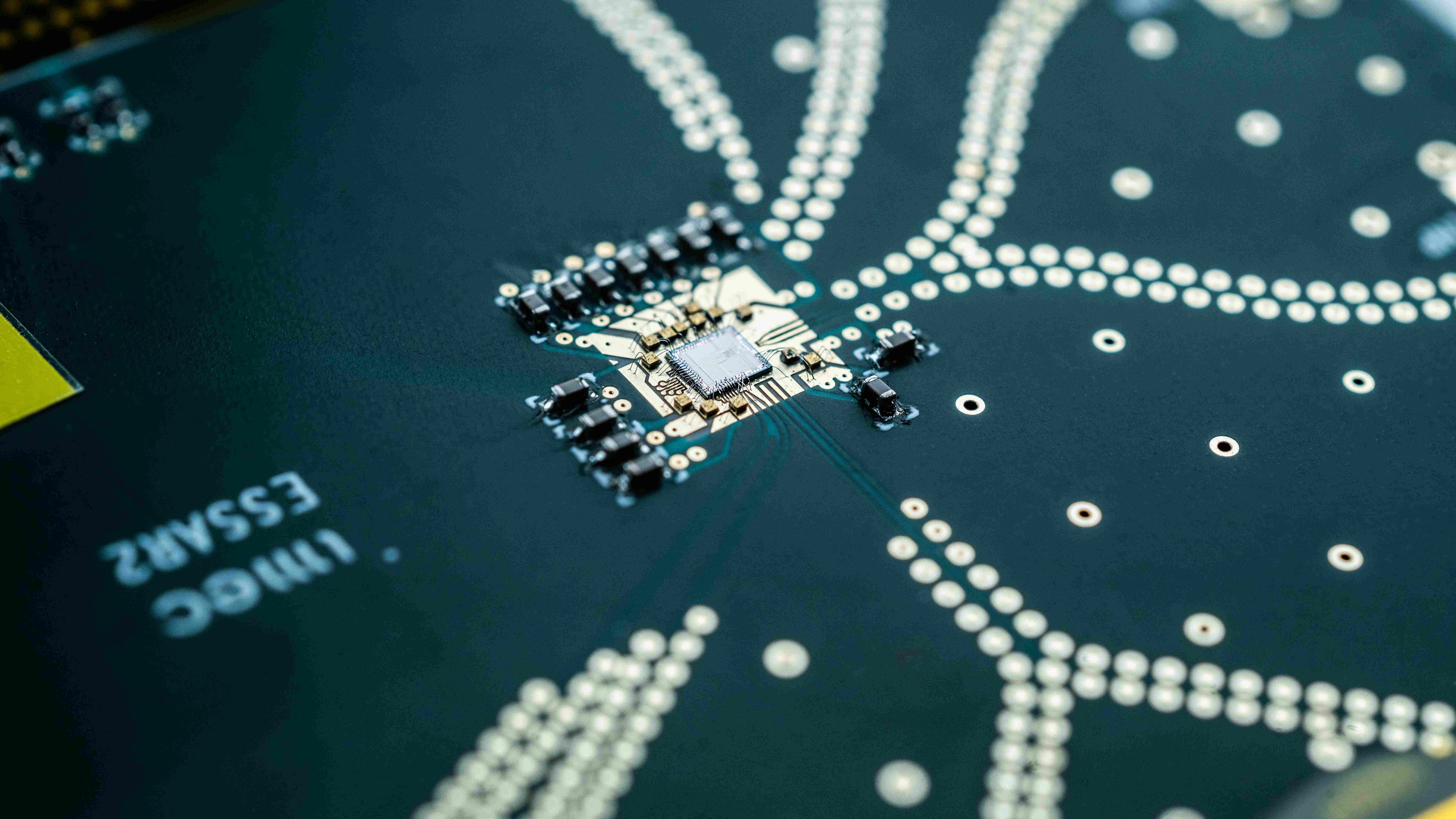
In analog components such as drivers and receivers, electronics that can generate signals above 100Gbaud used to be the domain of compound semiconductors such as InP. Imec focuses on various circuit techniques to achieve these speeds using mainstream SiGe BiCMOS, which offers advantages in terms of the complexity of functionality that can be integrated and manufacturing throughput.

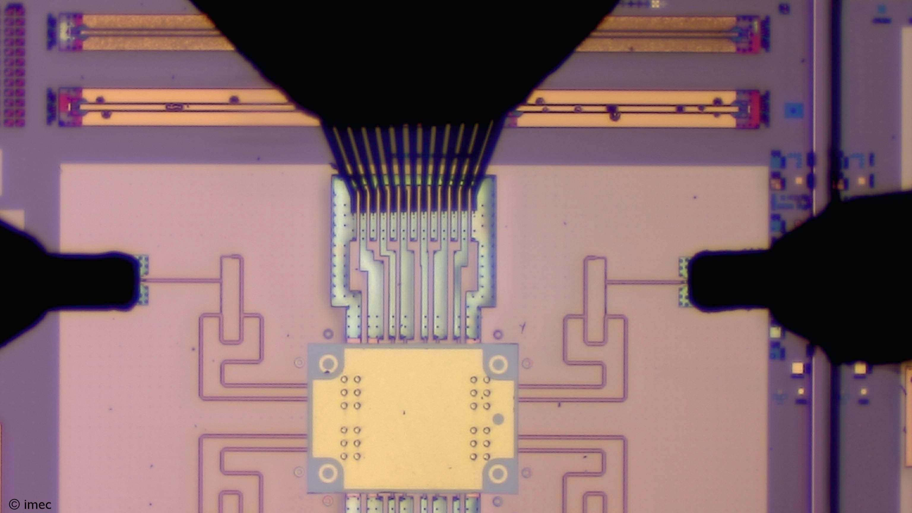
Silicon photonic transmitter and receiver test structures processed on iSiPP200
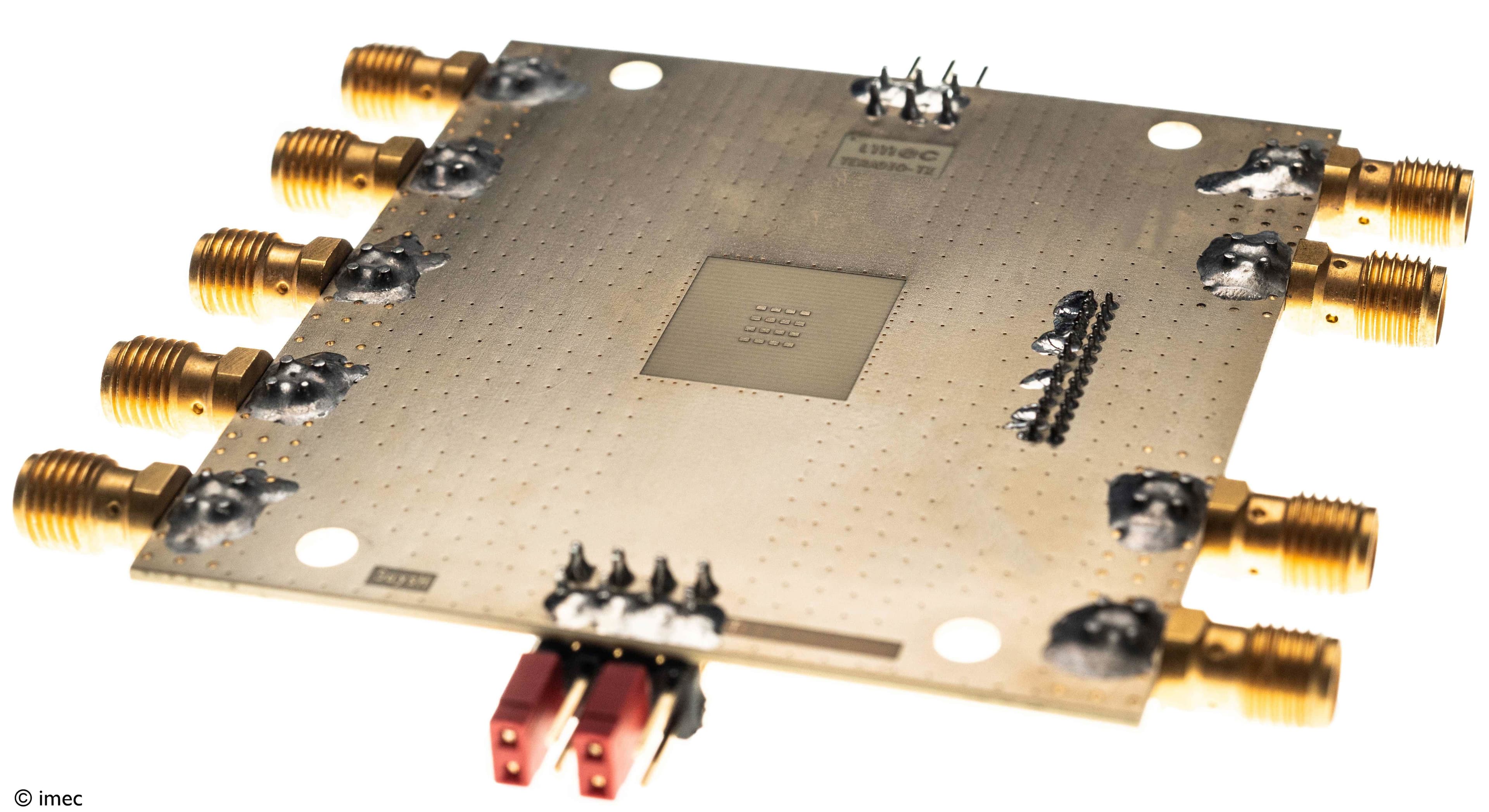
As an example, imec researchers made a 4-channel linear Mach-Zehnder modulator driver array in which they used traveling wave amplifier circuits to achieve very high bandwidths (around 90GHz). It was codesigned with a silicon photonic dual-polarization, IQ modulator. Another example is a 4-channel linear transimpedance amplifier array, also using traveling wave amplifier techniques, and achieving bandwidths as high as 60GHz. The amplifier was codesigned with the balanced Ge photodetectors, integrated on the silicon photonic platform.
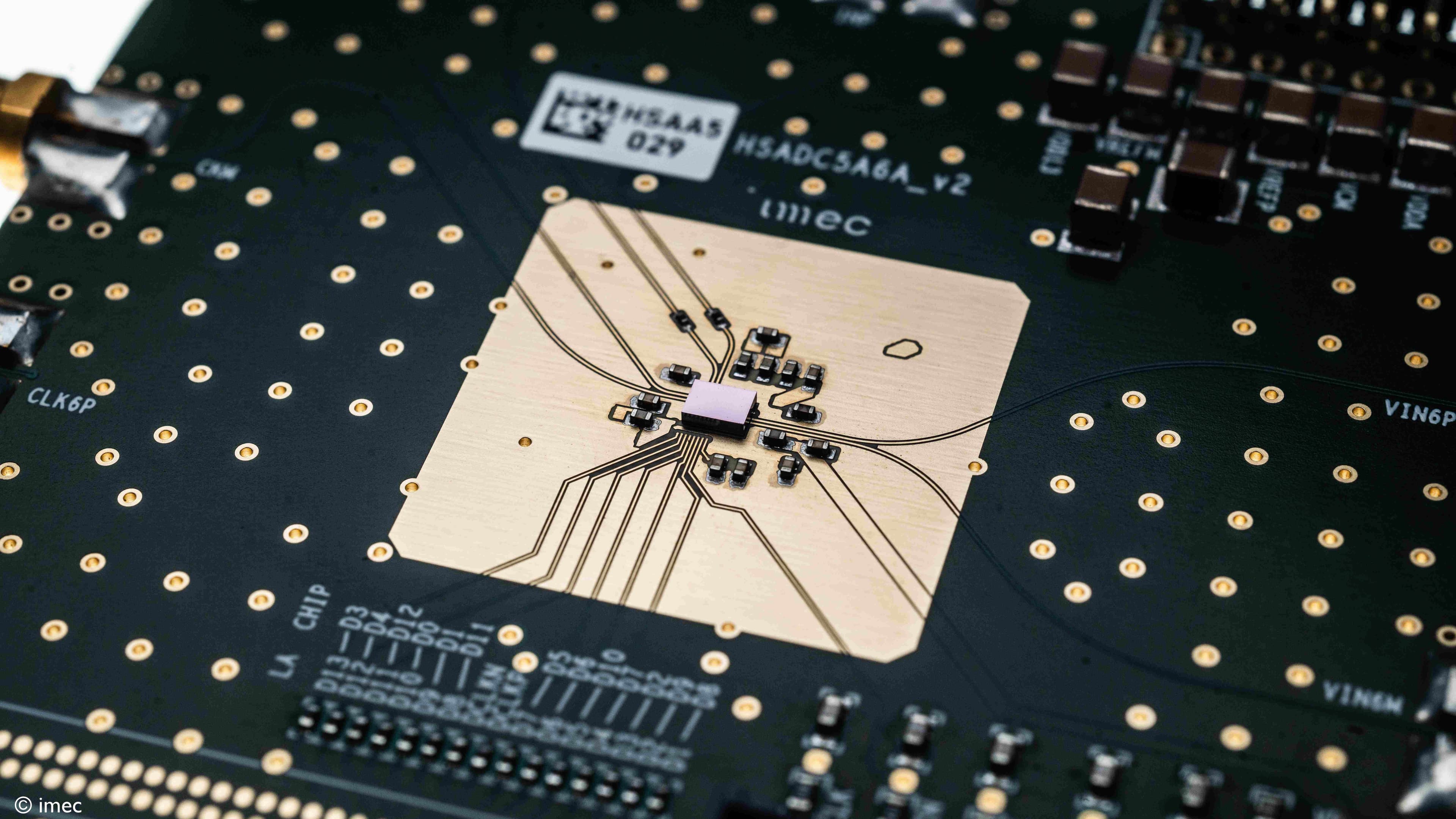
Just as for the opto-electronic frontend, also for the DACs and ADCs at least 60GHz bandwidth is needed for 100 to 130Gbaud operation. Such ultra-high-speed ADCs and DACS can be realized using scaled CMOS such as 5- and 3nm. Next to the bandwidth, also a low power consumption and small area are key. Imec is currently focusing on novel approaches for such high-speed wireline ADCs and DACs that overcome limitations in the existing state of the art. Designs of prototypes using 5nm CMOS are ongoing to validate the new concepts in the lab.
On the receiver side, research towards energy-efficient 100Gbaud PAM-4 clock and data recovery circuitry compatible with the new ADC approach is ongoing. Fractional oversampling is used in an effort to reduce the ADC sampling rate requirements. Feedforward and decision feedback equalization can be included to overcome impairments from the channel or bandwidth limitations on the optics.
To achieve the challenging specifications of next-generation high-speed transceivers, integration will obviously be key. This concerns both integration of chips and wafers from different material systems, each selected to provide optimum performance for the desired functionality, as well as integration to achieve the very high bandwidths necessary for beyond 100Gbaud operation. Heterogeneous integration is a key enabler to extend the functionality of imec’s silicon platform to integrate e.g. optical amplifiers and lasers. In collaboration with Sivers Photonics and ASM AMICRA, imec demonstrated the use of ultra-high precision alignment flip-chip processes to integrate InP optical amplifiers and lasers on its silicon photonic wafers. The alignment accuracy was better than 500nm and resulted in beyond 10mW waveguide coupled basic power.
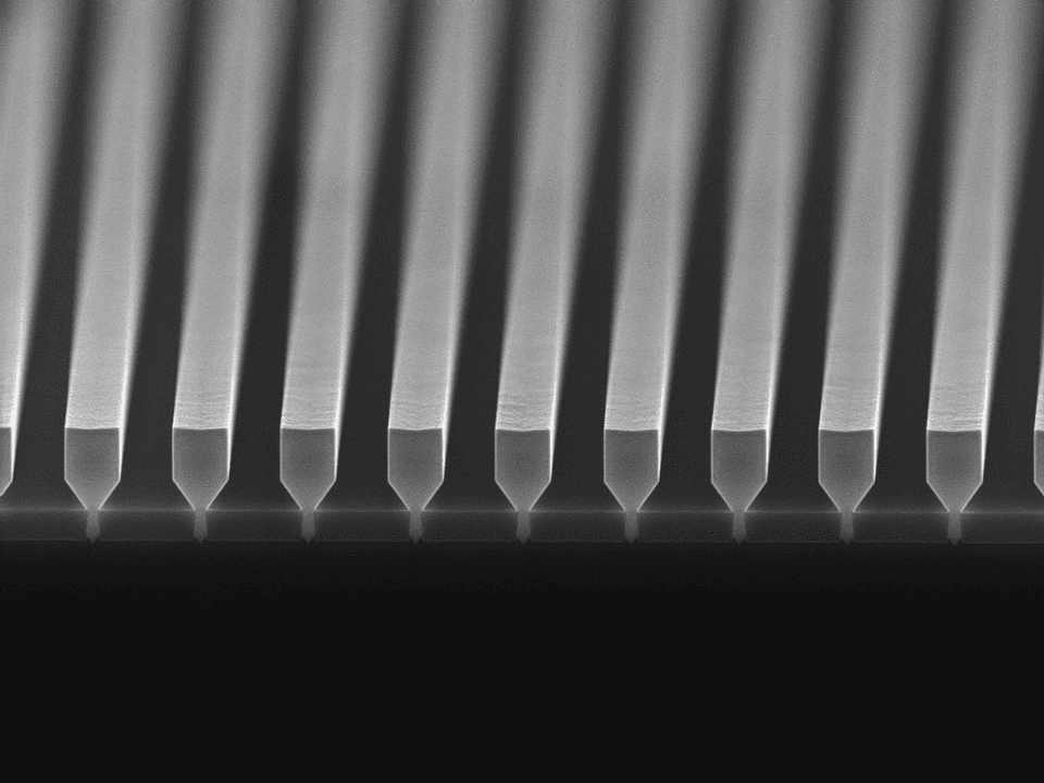
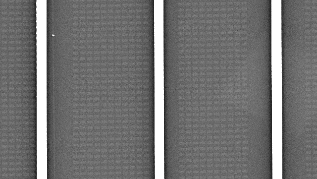
Micro-transfer printing is another approach to realize heterogeneous integration. It allows to integrate small components from almost any source material to almost any target substrate. It uses MEMS etch techniques to almost fully separate small chiplets from the donor substrate. Then, an elastomeric stamp with small posts is used to break the chiplets free from the donor substrate. Next, the stamp is used to deposit the chiplets onto the target substrate. Both of these operations require careful selection of the movement speed of the stamp. With this technique it is possible to deposit thousands of devices in a single step. In the H2020 Caladan project, this technique is further developed and used to realize GaAs quantum dot lasers and high-speed SiGe BiCMOS electronics.
Download this flyer for more info about micro-transfer printing.

Micro-transfer printing technique
Scaling far beyond 100Gbaud, e.g. towards 200Gbaud, may require innovative approaches beyond conventional transceivers, in which the functionality of electronics is shifted further into the optical domain. One example of such a device recently demonstrated by imec is an optical equalizer. This device can be understood by viewing a Mach-Zehnder modulator as an FIR (finite impulse response) or tapped delay line filter in the electrical input, optical phase output domain. The weight of each tap is related to the length (and drive voltage) of a particular section of the Mach-Zehnder modulator, while the FIR filter’s delays correspond to delays from the optical waveguides. Both of these can be readily manipulated: for example introducing a broadband time delay can be easily realized using a piece of optical waveguide. Even sign inversion (to realize more complex filter responses) is possible using waveguide crossings. This approach can be used to trade for example drive voltage of the modulator for improved bandwidth or can be tailored to introduce particular peaking in the electro-optic frequency response.
Want to know more?
-
Watch the webinar on this topic via this link.

Peter Ossieur received an M.Sc. Engineering degree in applied electronics and a Ph.D. in electrical engineering from Ghent University, Belgium, in 2000 and 2005, respectively. From 2005 to 2008, he was a Postdoctoral Fellow of the Fund of Scientific Research, Ghent University. During that time, his research was focused on 10Gbit/s burst-mode receivers and optoelectronics for automotive applications. In 2008, he became a part-time Professor of High-Frequency Electronics at the Faculty of Engineering, Ghent University.
In 2009, he joined the Photonic Systems Group, Tyndall National Institute and the Department of Physics, University College Cork, Cork, Ireland, where he became Senior Staff Researcher in April 2013. In this position he established an IC design group focusing on opto-electronic applications. In October 2017 he joined IDLab, an imec research group at Ghent University, as Senior Researcher and is currently Program Manager High-Speed Transceivers. He leads research activity focused on the development of high-speed analog and mixed-signal integrated circuits for photonic applications. He has (co-) authored 120 peer-reviewed papers, and holds several patents in the aforementioned research areas.
Published on:
24 May 2022


