This article was originally published on Technology Networks.
Technology to understand the brain
The idea of interfacing with a living brain has fascinated scientists for centuries. From surface electrodes such as EEG (electroencephalography) and ECoG (electrocorticography) to brain-penetrating neural probes, neurotechnology aims to understand the brain, map its cells, and even control and repair its functions. In this quest, devices to record brain activity and/or electrically stimulate the brain have proven instrumental.
Recording or stimulation devices, whether they are located on the surface or deep in the brain, are based on arrays of electrodes. Arrays for deep-brain recordings are usually arranged along a thin, elongated probe shank. In contrast, surface electrodes are arranged in grids placed directly on the brain surface (ECoG) or scalp (EEG). The higher the electrode density, the more fine-grained the recordings will be. And, the more electrodes, the more brain tissue is covered. This would allow researchers to capture the activity of individual neurons and pinpoint the exact location, which is essential for mapping the activity of specific brain regions and understanding underlying brain functions. Designing such high-density devices presents challenges regarding area, power, and noise.
The introduction of CMOS technology has revolutionized neural devices, enabling dense electrode arrays and high channel counts. Still, the quest for even higher channel counts persists, with the aim of unraveling the most complex neural enigmas. Additionally, integrating modalities other than recording, such as electrical stimulation of neurons, into the same device would open up new possibilities for understanding and manipulating neural circuits. Surpassing the current density limits will require a holistic approach, encompassing advanced monolithic integration and system-level innovations.
Here, we report the latest advancements in neurotechnology that will be presented in three papers at the 2024 VLSI conference. The first two papers demonstrate how clever circuit techniques enable smaller devices with high electrode counts and extensive coverage for brain-surface electrodes and deep-brain probes. The third paper shows an innovative front end that can tolerate large electrical artifacts -such as the ones resulting from electrical stimulation- on a small area.
A high-density readout IC for large-scale brain surface recordings
By placing electrodes directly on the surface of the brain, (micro-)electrocorticography (µECoG) enables researchers and clinicians to monitor and map brain activity. Because the electrodes record closer to the neural sources than EEG (where electrodes are placed on the scalp), it can provide more precise localization of brain activity, which is essential for high-definition brain mapping and emerging neural prosthetics.
However, implementing μECoG arrays with large brain surface coverage and high resolution remains challenging as each electrode must be wired out individually to map the brain activity's precise location accurately. This introduces practical challenges related to the bulkiness of wire bundles and transcutaneous connectors, and the readout integrated circuit (IC), a specialized electronic device designed to interface with and amplify neural signals recorded by the electrode array. Active µECoG arrays have partially tackled these limitations by integrating transistors into the flexible electrode grids, allowing for the multiplexing of many electrodes into a few data lines. However, existing readout ICs that are compatible with multiplexed inputs still have limited channel counts (max. 256) and insufficient bandwidth to record single-neuron activity.
Imec researchers propose a compact neural readout IC for high-resolution, large-scale µECoG arrays that can capture brain-surface activity with single neuron precision. The novel circuit architecture addresses two key challenges of dense electrode arrays: electrode DC offset and energy consumption. Electrode DC offset is a constant baseline voltage that develops at the electrode interface. These voltages are problematic because they superimpose on the brain signal and can saturate the recording channel. Each electrode has a different offset, which makes it challenging to multiplex. The proposed architecture keeps track of the offset in each electrode and cancels it, all while keeping the power consumption to a minimum. This is crucial for high-density arrays since power-hungry electrodes generate heat.
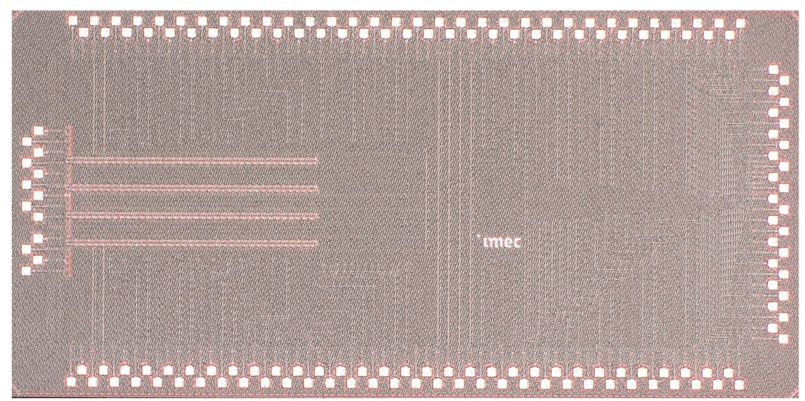
The IC is implemented in 22nm CMOS technology and records from 3,072 electrodes via 96 multiplexed channels, where one channel registers signals from 32 electrodes. Each multiplexed channel occupies only 0.0136mm2 and consumes 14.02μW.

The 3,072-channel μECoG readout IC for multiplexed channels. Each channel features a two-step incremental I-SAR-ADC (architecture on the right) that energy-efficiently cancels out electrode DC offset.
Record-high channel count for imec’s newest neural probe(1)
While ECoG is ideal for monitoring broad brain activity and mapping cortical functions with high spatial resolution and minimal invasiveness, intracortical implants such as imec’s state-of-the-art Neuropixels probes, provide an even more detailed and precise recording of neural activity at the level of individual neurons. Intracortical implants offer, for example, the granularity needed to decode complex neural signals and drive precise brain-machine interfaces for restoring motor function and communication in individuals with neurological disorders. The more complex the applications, the louder the call for even higher channel counts.
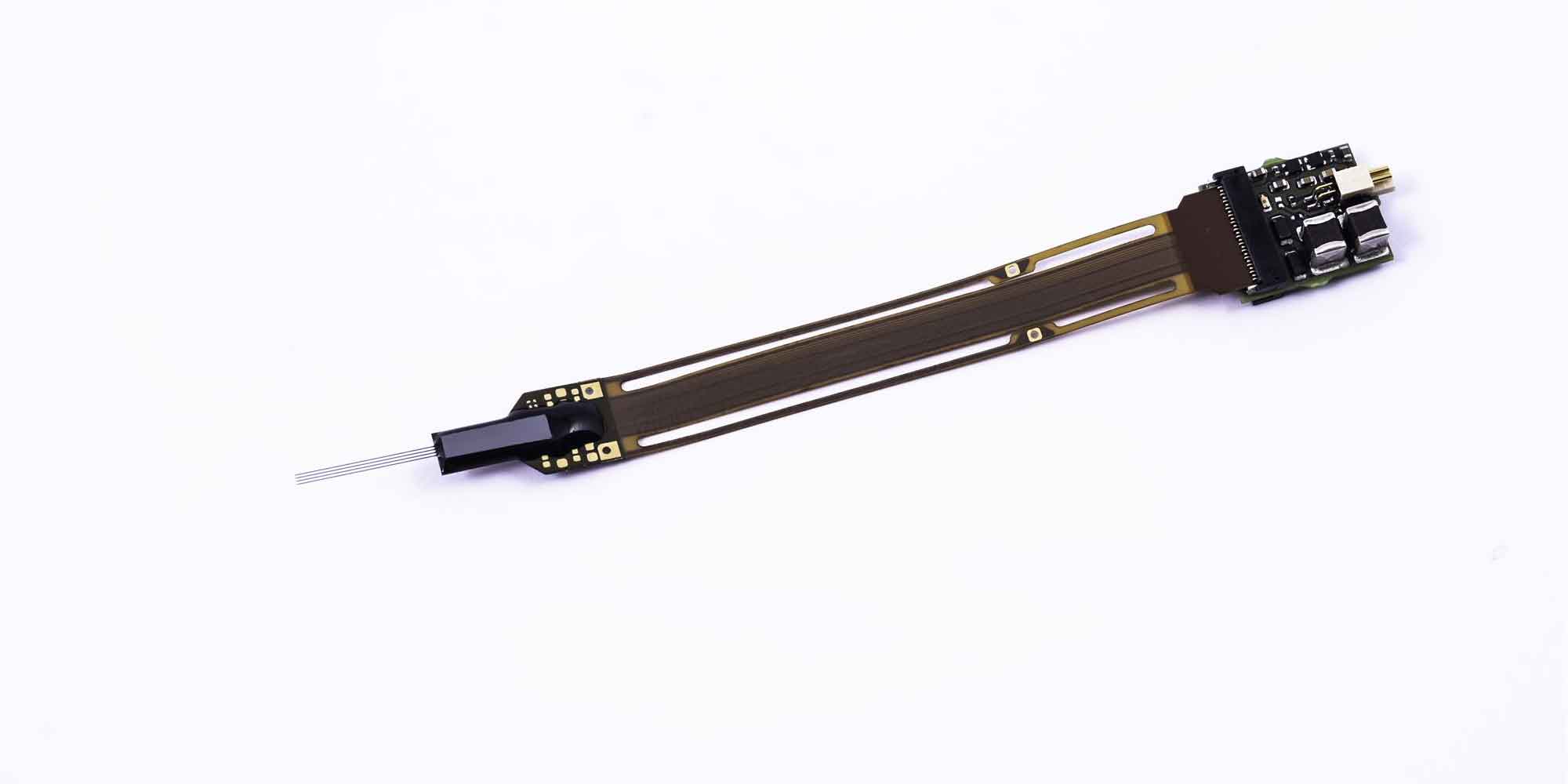
While current neuroprobes already boast record-high channel counts (384 recording channels for Neuropixels), the new neural probe prototype surpasses them with 5,120 electrodes on four implantable shanks and four times more readout channels (1,536) on the same probe base area. The probe outperforms current state-of-the-art designs thanks to circuit-level innovations by achieving 22 percent lower noise, 4.1 times smaller channel area, and 4.6 times lower channel power, setting a new benchmark for neural recording technology. Moreover, this latest prototype is fabricated using 55nm 9-metal-layer CMOS technology, followed by a fab-compatible 300mm-wafer process. The probe enables high-quality recordings with unprecedented resolution and coverage of brain activity that will provide a more detailed understanding of the brain and propel neuroscience forward.
Aside from the work on the silicon probe itself, the imec researchers also made further improvements in miniaturizing the whole system and packaging. The introduction of capless LDOs (low dropout regulator) and a custom low-power LVDS (low-voltage differential signaling) interface that streamlines data transmission was instrumental. An LDO generates the supply voltage to the chip and normally requires external capacitors to maintain a stable voltage. The packaging can be made smaller by removing the capacitors (‘capless’) and thus the number of external components. The capless LDOs employ circuit techniques to ensure a stable operation.
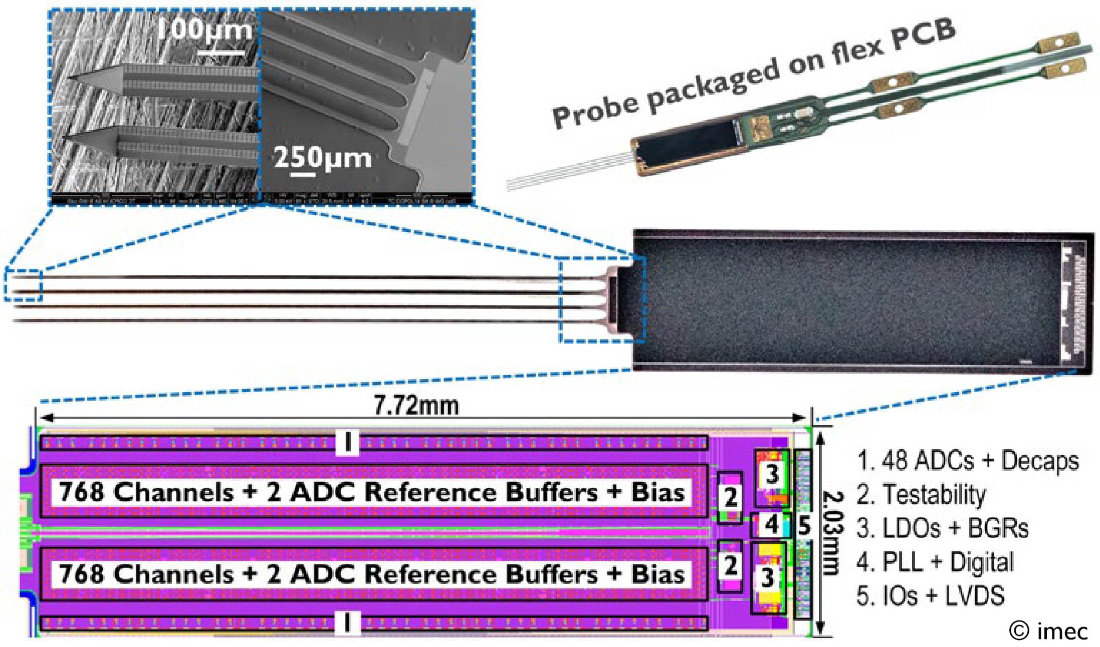
The silicon neural probe prototype and packaging, and the high-level layout overview. The probe monolithically integrates four implantable shanks and a non-implantable base.
A new technique suppresses stimulation artifacts in recording electrodes
In parallel with efforts to create high-density recording devices, researchers are also investigating ways to combine recording with other modalities, such as electrical stimulation. The combination of recording and electrical stimulation forms the basis of neuroscience studies, prostheses, or spinal cord injury treatments and epilepsy. One significant remaining challenge is achieving electrical stimulation while recording neural activity. The stimulation pulse causes artifacts or common-mode interferences that saturate the recording amplifiers, resulting in signal clipping and loss of information.
Imec now designed a low-noise analog front-end (AFE) with a new common-mode suppression technique that tolerates 400mVpp common-mode interferences while being able to capture single-neuron signals. The so-called common-mode feedback suppression loop works by first monitoring the output of the recording channel for artifacts and subsequently feeding that information back into the inputs of the channels. This allows the system to adjust the recording process in real time and cancel out the artifact. The technique can efficiently handle common-mode interferences over a hundred times larger than the actual neural signals and over multiple channels simultaneously.
Imec demonstrated a 16-channel AFE prototype that tracks artifacts across multiple channels and cancels them out in groups. The prototype system, featuring a small area (0.006mm2 per channel) and low power (3.1µA), effectively reduced interferences without consuming excessive resources, such as area or power. The additional area and power from the common-mode suppression loop were almost negligible.
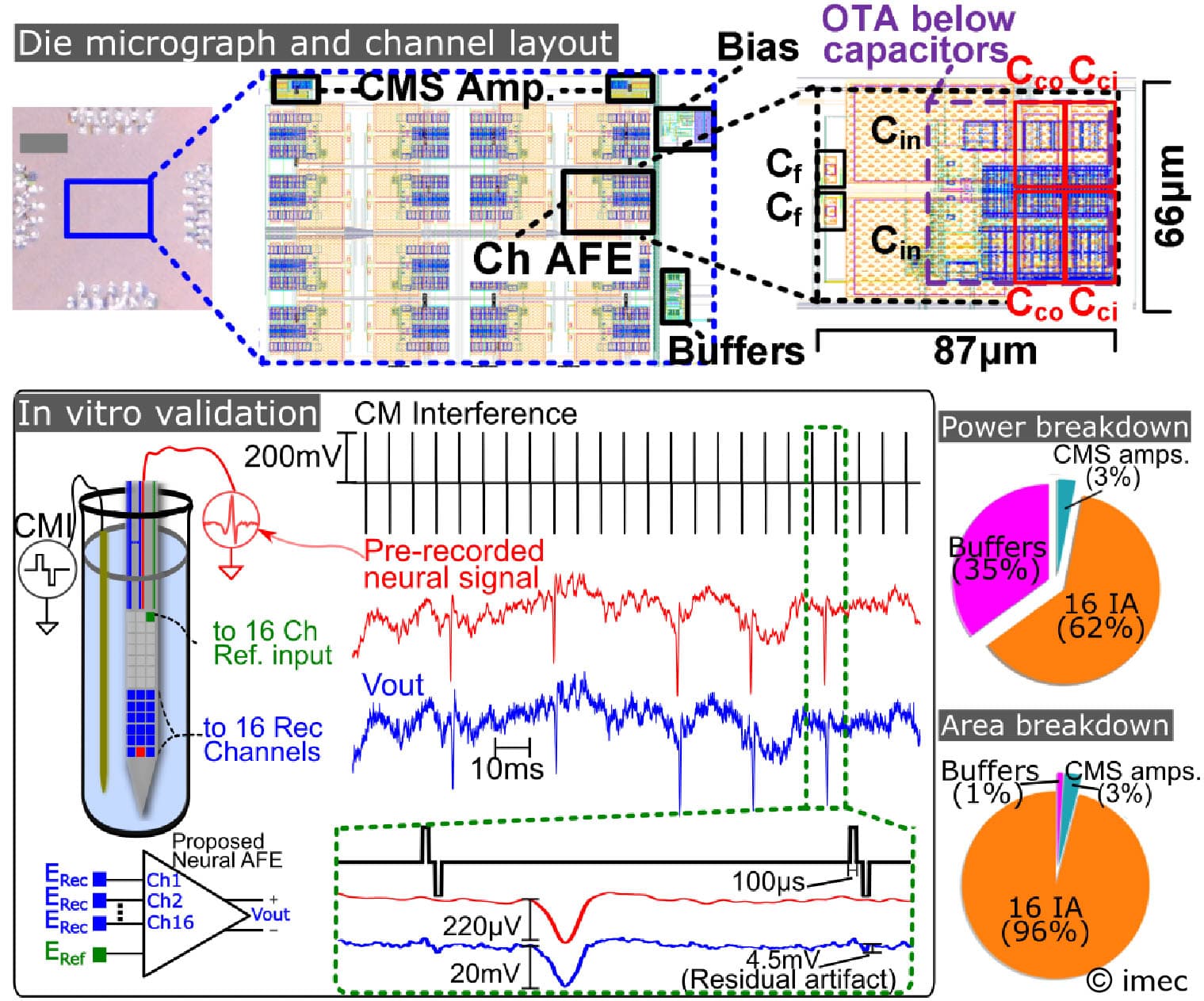
(Top) AFE with channel layout. (Bottom) Saline experiment to confirm the effectiveness of the common-mode suppression technique. The prototype picks up common-mode artifacts and a pre-recorded signal. The measured signals demonstrate negligible residual common-mode interference.
(1)This research was partially supported by the NIH grant 1U01NS115587 (Neuropixels NXT).
Want to know more?
This article is based on three papers that will be presented at the 2024 VLSI conference:
- X. Huang, X. Yang, A. Lodi, C. Van Hoof, G. Gielen, C. Mora Lopez (2024). A 3072-Channel Neural Readout IC with Multiplexed Two-Step Incremental-SAR Conversion and Bulk-DAC-Based EDO Compensation in 22nm FDSOI. In: 2024 IEEE symposium on VLSI technology & circuits, June 2024, Honolulu, Hawaii.
- X. Yang, J. Aymerich, P. Coppejans, W. Hsu, C. Sawigun, J. Cisneros Fernandez, A. Lodi, M. Caceres Rivera, B. Tacca, M. McDonald, H. Mahmud-UI, B. Dutta, J. Putzeys, C. Mora Lopez. A Highly-Integrated 1536-Channel Quad-Shank Monolithic Neural Probe in 55nm CMOS for Full-Band Raw-Signal Recording. In: 2024 IEEE symposium on VLSI technology & circuits, June 2024, Honolulu, Hawaii.
- J. Aymerich, C. Sawigun, J. Cisneros-Fernandez, X. Yang, C. Mora Lopez. A 16-Ch CMI-Tolerant Neural AFE with Inherent CM Detection and Shared CM Suppression Achieving 0.006mm2/Ch and 3.1μW/Ch. In: 2024 IEEE symposium on VLSI technology & circuits, June 2024, Honolulu, Hawaii.
Consult imec’s webpage for general information about neural probes

Carolina Mora Lopez received the Ph.D. degree in electrical engineering from KU Leuven, Leuven, Belgium, in 2012, in collaboration with imec, Leuven. From 2012 to 2018, she worked as a Researcher and an Analog Designer with imec focused on interfaces for neural-sensing applications. She is currently the Scientific Director and the Team Leader of the circuits for neural interfaces team with imec. Her research interests include analog and mixed-signal circuit design for sensors, bioelectronics, and neural interfaces. Dr. Mora Lopez is an IEEE SSCS Distinguish Lecturer and serves on the Technical Program Committee of the VLSI Circuits Symposium, International Solid-State Circuits Conference (ISSCC), and ESSCIRC conferences.
Published on:
24 June 2024


