Atomic-scale bottom-up fabrication: Area-Selective Deposition (ASD) of Si-based dielectrics and its application in IC manufacturing
Master projects/internships - Leuven | More than two weeks ago
In depth fundamental understanding of atomic layer deposition (ALD) of dielectric materials and surface chemistry to enable innovative and technologically relevant solutions for nano-electronic component miniaturization
As we approach the limits of scaling devices, novel architectures are needed in order to meet the demand of a smaller transistor footprint while maintaining high performance and low power. For nodes beyond the 5 nm regime, several options have been proposed. The common theme in these approaches is to go from a horizontal to vertical and three-dimensional (3D) architectures. As an example, a Complementary Field Effect Transistor (CFET) architecture, where NMOS and PMOS devices are vertically stacked and are controlled using a common gate, would result in maximum device footprint reduction.
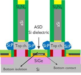
There are many challenges associated with the implementation of these novel architectures, such as the thickness uniformity control of the dielectric insulation in the current approach based on dielectric etch back. In this case, the area-selective deposition of a Si-based dielectric layer on metals such as Ru, W, Mo or Co by topographical deposition or surface-driven atomic layer deposition (ALD) represents a clear asset. The selective organic passivation of the Si nitride non-growth area has a key role to achieve a successful selective process when combined with a low temperature ALD SiOx process.
The final goal of this project is to treasure all the learning gathered on un-patterned surfaces to nano-scale 3D features where the growth and selectivity mechanisms are expected to be different with respect to planar surfaces, due to different incoming surface composition (after etching and post-etching clean) and due to topography/geometry effects.
A great asset offered by Imec is the possibility of getting sub-20 nm patterned features as a result of cutting-edge technology, integration and state-of-the-art materials and 300 mm IC manufacturing equipment.
A cross-team collaboration between the surface and interface preparation, thin film deposition and characterization experts will enable and in-depth understanding of material properties and mechanisms.
Required background: Master in Materials Science, Materials Engineering, Nanotechnology, Chemistry, Physics, Chemical Engineering or Electrical Engineering.
Master program: Chemistry/Chemical Engineering
Type of work: 10% literature study, 90% experimental work (depending on the interest of the student a combined experimental/theoretical investigation might be possible)
Type of Project: Combination of internship and thesis
Duration: 6 - 12 months
Supervisor: Annelies Delabie (Chemistry, Nano)
For more information or application, please contact Silvia Armini (silvia.armini@imec.be)
Only for self-supporting students.