Intro
With pioneer works starting in the late 1980’s, the road towards EUV infrastructure development and readiness has been a challenging one. Although EUV lithography has a number of similarities to, e.g., 193nm optical lithography, it presents unique characteristics. For example, with a short imaging wavelength of 13.5nm, EUV radiation is not transmitted through ambient air and is strongly absorbed by all solid materials. Challenges to EUV development included for example the light source (with sufficient power to enable cost-effective production), mask inspection and defectivity, and photoresist issues.
The successful integration of EUV lithography into semiconductor manufacturing would however bring many benefits. For example, the ability to print features with single exposure EUV lithography instead of with multi-patterning 193nm lithography leads to enhanced process simplification and reduced cost per wafer. This has driven the semiconductor industry to continue improving on the scanner, source and mask infrastructure.
In recent years, significant progress has been made for all critical issues. For example, with a recent power demonstration of 250W, the light source now has shown capability to meet the roadmap target and ensure sufficient throughput in terms of wafers per hour. First insertion of EUV lithography in high-volume manufacturing is expected in the critical back-end-of-line (BEOL) metal and via layers of the foundry N7 logic technology node (with metal pitches in the range of 36-40nm), in the 2018-2019 timeframe.
Exploring the options for N5 and beyond
In the meantime, imec and its partners are weighing the options for the following node (32nm pitch and below). At these dense pitches, various patterning approaches are being considered that differ in terms of complexity, wafer cost, and time to yield. These approaches include variations of EUV multi-patterning, hybrid EUV and immersion multi-patterning, and EUV single exposure. Last year, at the 2017 SPIE Advanced Lithography Conference, imec presented many advances in hybrid multi-patterning (hybrid 193i-EUV) by combining, e.g., 193nm immersion-based self-aligned quadrupole patterning (SAQP) of 32nm pitch metal lines with a direct EUV print of the block layers.
At the same time, imec has been pushing the limits of EUV single exposure for logic and memory technology nodes, as further benefits can be expected from a single exposure step in terms of process simplicity, wafer cost and time to yield. For example, imec calculated a 20% reduction in wafer cost when transitioning from an all 193nm immersion-based solution to a solution where blocks and vias are patterned with EUV single exposure. A further 3.2% reduction is expected for EUV single patterning of the critical metal lines and vias. Equally important is time-to-yield, which heavily depends on process complexity. The example of the figure below shows a reduction in roughly 60% required process steps for the hybrid 193i-EUV technique when compared to the all immersion-based solution, and roughly 80% with EUV single exposure. This can translate to days or weeks reduction in the turn-around time for a single wafer lot. Considering a very large number of lots are required to develop a technology, this can result in a significant advantage.
(Left) Benefits of using EUV lithography single exposure in terms of wafer cost and (right) process simplicity
Yet, several challenges still need to be tackled before these small and dense features can be patterned with EUV single exposure. Despite tremendous progress, critical issues remain with respect to e.g. the resist performance, stochastic failures, photomask, metrology and inspections and pattern transfer. In addition, a more fundamental understanding of the critical EUV processes, such as the resist reaction mechanisms, is still lacking. At the 2018 SPIE Advanced Lithography Conference, imec has demonstrated promising advances in all these areas, focusing on two primary use cases: the logic N5 32nm pitch metal-2 layer, and 36nm pitch contact holes for dense DRAM applications.
EUV stochastic printing failures: limiting the applicability of EUV lithography
The term ‘stochastic effects’ refers to random, local variability that occurs between structures that should in principle print identically. These effects have always been part of lithography. Best known is critical dimension (CD) variability, which is quantified through metrics such as line-width roughness, line-edge roughness or local CD uniformity. Over the years, these metrics have been intensively studied. However, next to CD variability, stochastic effects can give rise to local, random failures such as micro-bridges and broken lines (when printing lines/spaces), or bridging contacts and missing contacts (when printing contact arrays). These failures are less understood. They are typically generated throughout the complex resist-pattern-formation process itself. Now that dimensions are shrinking and less photons are available during EUV exposure compared with traditional 193nm (immersion) lithography, these failures are expected to increasingly impact the yield of future devices.
Stochastic printing failures observed after printing (top) lines/spaces, and (bottom) contact holes.
To gain more fundamental insights, imec has continued its systematic study of stochastic failures, for both lines/spaces and contact arrays. The team focused on the quantification of the stochastic failures and investigated their dependency on experimental parameters (such as dose, resist, CD). The final goal was to understand how these stochastic effects limit the applicability of EUV lithography, and to identify the knobs that allow minimizing the number of failures.
The new method for quantifying the stochastic printing failures consists in automatically counting the relative number of failures (i.e., the missing and bridging contacts, and the line breaking and micro-bridges) that are visible in a series of SEM images. Although this SEM-based technique can only be applied to a limited inspection area, the method is ideally suited for determining the process parameters affecting the number of stochastic failures.
The number of stochastic failures is found to depend on many experimental parameters, providing several knobs for optimization. For example, it largely depends on target CD (line or space), or on the target diameter of the contact hole. E.g., micro-bridges and missing contacts are more abundant as the width of the space or the size of the contact is smaller. This behavior also varies with pitch: for dense pitches, the number of missing (and bridging) contacts increases rapidly as the size of the contacts becomes smaller (or larger). These stochastic failures limit the available CD-window – the CD-range for which neither type of printing failure is observed – and hence the applicability of EUV lithography.
Example of the impact of failure mechanisms on the available target CD-range for dense lines/spaces (36nm pitch). Exposure dose was at ~32mJ/cm2.
Importantly, the amount of stochastic failures also has a strong dose dependency: with increasing exposure dose, the number of failures decreases significantly. This implies that exposure dose is a very important knob for reducing the number of stochastic failures. In recent years, resist vendors have been optimizing resists for enhanced resist sensitivity. This way, the resist exposure dose could be reduced close to the cost-effective target of 20mJ/cm2, as to guarantee sufficient wafer throughput. Our findings, however, call for using larger exposure doses as a way to mitigate the stochastic printing failures.
Characterization of the resist performance: introducing new metrics
Over the years, imec, in collaboration with many materials partners, has assessed different resist materials strategies, including chemically amplified resists (CARs, originally developed to work with optical lithography), metal-containing resists and sensitizer-based resists. For most of these materials, comparable performance improvement in terms of resist resolution has been achieved. And the knobs have been identified to enhance the resist sensitivity, and as such enabling more efficient absorption of EUV light.
At the 2018 SPIE Advanced Lithography Conference, imec introduced a comprehensive way of characterizing EUV resists. As an illustration, the characterization was applied on 32nm dense line/space patterns and on 36nm dense contact hole pitch, for chemically amplified resists. New types of metrics were introduced to judge the quality of the pattern. To quantify resist roughness on resist lines, the imec team used ‘power density spectrum’ (PSD) as a new metric to compare different resist processes. This metric is complementary to the traditional metrics based on scanning electron microscopy (SEM) with the benefits of removing the SEM noise (unbiased resist roughness) and looking at the variance of the variable (linewidth for LWR, line edge position for LER) per unit frequency. Frequency is one over length, so that high frequencies represent short line length scales and low frequencies represent long line length scales. The team also introduced the metric for counting stochastic printing failures, as to provide an early stage assessment on the patterning fidelity of the examined resists at low, mid and high exposure dose. By using all the metrics, a lithographic performance comparison has been made between various resists. Two positive tone chemically amplified resists have been identified at the exposure dose of 45mJ/cm2 and 33mJ/cm2 for logic (pitch 32nm dense line/space) and for memory (pitch 36nm dense contact holes) use cases, respectively.
Pitch 32nm line-space: power spectrum density, unbiased LWR and failure analysis for low, mid and high exposure dose EUV chemically amplified resists.
Pitch 32 dense line-space patterning and pitch 36 dense orthogonal contact hole patterning in single EUV exposure (at 45mJ/cm2 and 33mJ/cm2 exposure dose, respectively, on ASML NX3300 EUV scanner tool)
Resist smoothening by post processing: a novel approach
Right after resist exposure and development, post-processing techniques are applied to further smoothen down the resist lines. Imec, in collaboration with etch tool vendors and material suppliers, has proposed new approaches to smoothening, providing encouraging initial results for dense features. In the study, the team focused on 32nm pitch lines/spaces (16nm half pitch (hp)), but the approach can be extended to dense contact holes and pillars.
With the further down-scaling of dimensions, the gap between achievable smoothening (expressed e.g. in terms of line-edge roughness) and the required target is getting increasingly larger. And this makes smoothening of 16nm hp resist lines very challenging. For example, at these small dimensions, the height of the photoresist lines after litho and development is becoming very small (typically 25 – 27nm), leaving very little budget for patterning the underlying layers. Also, top roughness, and defects such as footing, scumming, line interruption and non-bridging are playing an increasingly important role. These roughness and defects are transferred down during subsequent process steps, impacting the device performance.
Imec has first set up a baseline process for chemically amplified and metal-containing resists, allowing to determine the initial process parameters in terms of line-edge roughness, line-width roughness and line CD. Then, various etch approaches (including e.g. direct current super-position and quasi-atomic layer etching) are explored and the knobs are identified that lead to optimized resist smoothening. Although continued optimizations are being done, reductions in post-etch roughness with these techniques have shown roughly 20-30% improvement when compared to a conventional etch technique.
The imec team is also investigating alternative smoothening paths, such as stack optimization. Here, it is investigated how changing the layers underneath the resist (such as photoresist under layer, mask or oxide) impact the etch process and mitigate roughness. Besides stack optimization, novel techniques such as plasma-based smoothening and photoresist encapsulation are being explored. Importantly, new metrology such as power density spectrum and 3D-AFM have been introduced and further developed to optimize resist assessment before and after smoothening.
Computational litho techniques: the benefits of using SRAFs and retargeting
Resist materials advances alone are not sufficient to meet the requirements of EUV lithography single patterning. Imec has also focused on co-optimizing the photomask, film stack, EUV exposure and etch towards an integrated patterning flow to achieve full patterning of the structures. The team also explored the use of advanced computational lithography techniques to improve the patterning of a metal-2 logic layer.
For this metal-2 layer, source optimization (i.e., the optimal illumination setting of the scanner to print this clip), optical proximity correction (OPC) model calibration and OPC have been performed using Tachyon computational lithography software.
To optimize the printing of 32nm pitch lines/spaces, imec has explored the use of design-for-manufacturing (DfM) techniques, i.e. sub-resolution assist features (SRAFs) and retargeting. With SRAFs, specific features (such as scattering bars) are added at mask level, that do not print onto the wafer but do help enlarging the process window for the target features. With retargeting, the original line width or space is changed to enlarge the process window. For example, isolated features are printed wider in order to reduce the number of defects. The team applied the techniques on a traditional dark field mask with positive tone photoresist.
The use of both SRAFs and retargeting was found to have a number of advantages. First, when using SRAFs, experimental data showed an increased exposure latitude (EL) and depth-of-focus (DoF, the range of focus that keeps the resist profile of a given feature within all specifications for a specified exposure range). Next, applying retargeting increases the defect-free CD process window for printing logic structures as shown in the figure below. And finally, the techniques allow to print metal line tip-to-tips more uniformly (i.e., with regular CD) across different feature types.
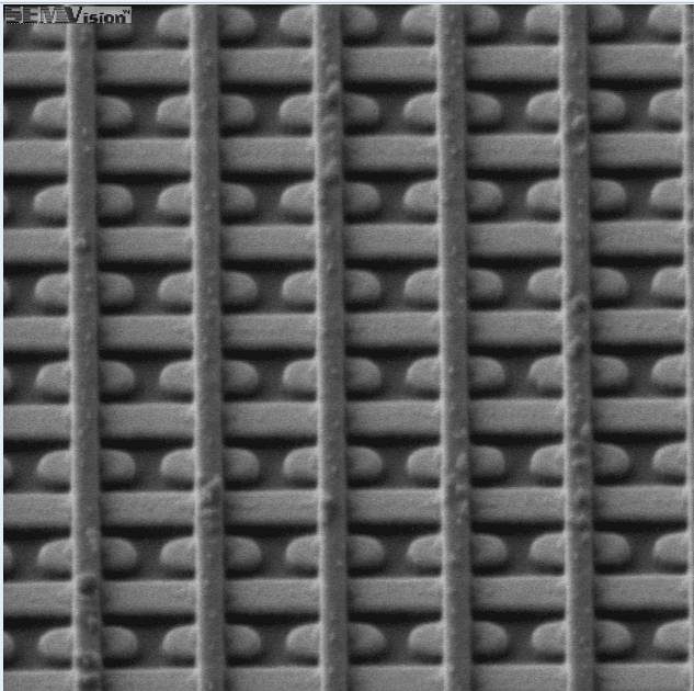
SEM image of a metal-2 logic pattern after litho using retargeting. Note different CD’s for isolated and dense features.
Wafer data showing increased EL and DoF when SRAFs are applied on typical structures within the logic
Conclusion
Imec, together with its partners, is exploring various options to optimally enable and implement EUV lithography. In this work, imec has pushed the limits of single exposure EUV for printing critical 32nm pitch metal layers and 36nm pitch contact holes. This has been achieved through an increased understanding and optimization of various contributors – including resist performance, stochastic printing failures, photomask, metrology and inspections, and pattern transfer. The ability of EUV to do single patterning is expected to have a big impact on the roadmap and cost of near-term technology nodes.
Want to know more?
- Read the press release 'Imec pushing the limits of extreme Ultraviolet Lithography single exposure for logic N5 metal layers and dense DRAM applications'
- First EUV lithography high-volume manufacturing solution for N5 BEOL, imec magazine, March 2017
Greg McIntyre is Director of Advanced Patterning at imec and responsible for areas related to advanced lithography equipment and process development, metrology and patterning process control, computational lithography, and exploratory patterning materials. Prior to joining imec, he was the technical lead for various areas of advanced lithography, imaging and modeling within the IBM research alliance in Albany, New York. He has published over 80 papers, won 7 best paper awards, and has launched a successful startup in the field. Prior to becoming a lithographer, Greg served as a Captain in the US Army. He holds a PhD and MS in Electrical Engineering from the University of California, Berkeley, and a B.S. from the United States Military Academy at West Point.

Peter De Bisschop has a PhD degree in Physics from Leuven University. He moved to imec in 1986, where he joined the lithography group in 1995. He worked on various topics related to exposure-tool-control and -qualification, imaging, masks, rigorous simulations, OPC, and DTCO. His focus in the past few years has been on stochastic effects in EUV.
Danilo De Simone holds a MS degree in Chemistry from the University of Palermo (Italy) and has 18 years of experience in semiconductor R&D, in the field of nanolithography. He led the development of lithographic materials for 90nm and 65nm NOR Flash devices for STMicroelectronics (STM) in Italy, and covered the role of assignee at STM Alliance in France and STM in Singapore. In 2008, he joint Numonyx to lead the R&D development for lithographic materials and first 32nm double patterning for PCM devices. In 2011, he moved to Micron Technology to introduce 45nm PCM devices in HVM, and to develop lithographic solutions for novel devices. In 2013, he joined imec, leading the research on photo materials for EUV lithography.

Frederic Lazzarino received his MSc degree in Material Science from Joseph Fourier University (Grenoble, France) in 2000. He obtained his PhD degree in Physics in 2005 (LTM-CNRS, Grenoble, France) and joined Crocus technology, an MRAM company, in 2006, after 1 year at ST Microelectronics (Crolles, France). After 2 years as an MRAM etch engineer, he became researcher at imec, specialized in back-end-of-line (BEOL) dry etch processing. He is currently principal member of technical staff and he leads the BEOL etch team.

Victor M. Blanco Carballo has an MSc degree in Physics and an MSc degree in Electrical Engineering from the University of Zaragoza and the University of Valladolid, and holds a PhD degree in Microelectronics from the University of Twente. He worked at Nikhef developing radiation sensors for high energy physics and later on moved to ASML working on various topics like immersion defectivity, throughput, customer yield improvement and EUV defectivity. In 2015 he joined the Advanced Patterning Center at imec working as a research engineer in the EUV patterning of BEOL layers.
Published on:
1 March 2018

