Imec’s solution includes two scenarios for EUV lithography insertion, as well as proposals for design rules, masks, photoresists, etching, metrology and variation assessment. In this article, one of these scenarios is described in more detail. It combines immersion-based self-aligned quadruple patterning with EUV lithography block patterning, to achieve metal layers with pitches as small as 32nm. To assess the platform’s suitability for high-volume manufacturing, the uniformity of the layers and their local variability is discussed.
The patterning of advanced logic back-end-of-line layers
As we move towards more advanced technology nodes, the patterning of critical back-end-of-line (BEOL) metal layers with ever more aggressive pitches (e.g. 32nm) has become very challenging. In these BEOL layers, typically, trenches are created which are then filled with metal in a final metallization step. In order to create a disconnection in the continuous trenches, block layers perpendicular to the trenches are added, resulting in small metal tip-to-tips. In the industry, various options are considered to pattern the most aggressive BEOL layers and blocks. One option is to use immersion lithography in combination with so-called self-aligned quadruple patterning (SAQP) for the metal lines, and triple patterning for the block layers. This option however requires a triple block mask and a triple litho-etch process flow, which adds to the cost and complexity of the proposed solution. Another option is to pattern the BEOL metal layers directly with EUV lithography (EUVL) in one single exposure. Although this direct EUVL integration flow is very simple and cost-effective, pattern fidelity (e.g. the shape of the pattern) and pattern variability, as well as mask making are expected to be extremely challenging, especially for very small tip-to-tips.
One of the alternatives imec is evaluating is a ‘hybrid’ option, in which immersion-based SAQP of metal lines is combined with a direct EUV print of the block layer – using ASML’s NXE:3300 scanner.
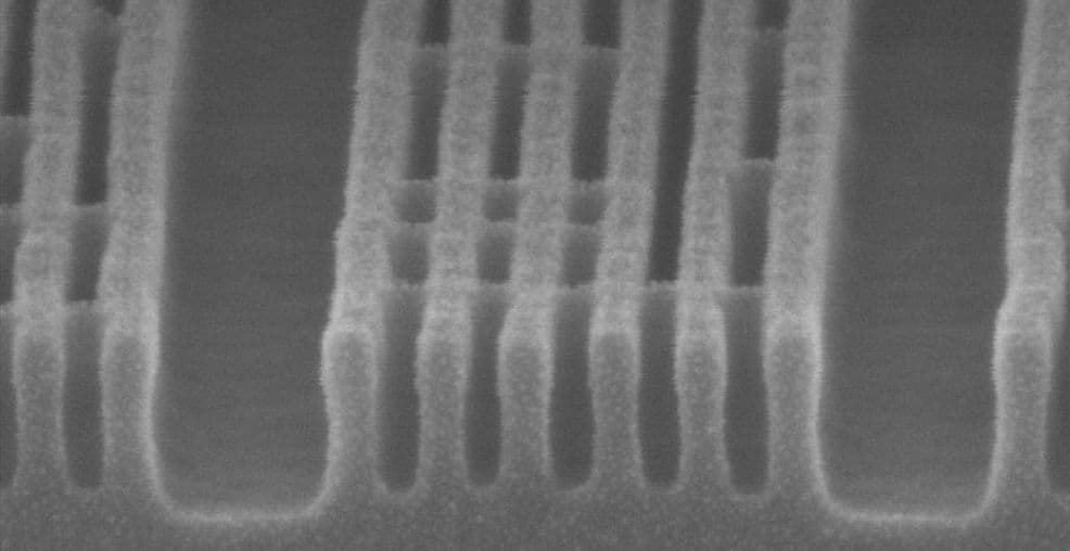
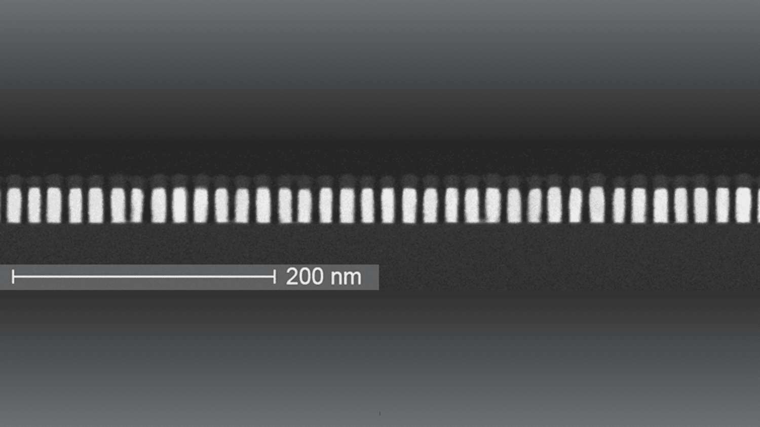
32nm pitch metal2 patterning through SAQP + EUV block (XSEM image)
The imec N7 (iN7) EUV platform
To evaluate the viability of this ‘SAQP + EUV block patterning’ option, imec makes use of its iN7 platform. This platform has been developed to evaluate EUV patterning of advanced logic BEOL layers. The platform considers two layers: metal1, with 42nm pitch, and metal2, with 32nm pitch and 7.5 track design. Via1 connects the two metal layers using a dual damascene process flow. With these aggressive pitches, iN7 corresponds to IDM N7 and foundry N5 requirements for the BEOL. The patterning of both metal1 and via1 can be achieved through EUV single exposure. The iN7 platform is used to evaluate the hybrid immersion/EUVL solution for patterning metal2.
Optimizing design rules, mask and etch process
Prior to printing and evaluating the pattern, considerable efforts and innovations were performed in various litho-related areas. First, imec developed compliant design and design rules to support the possible patterning schemes. Also, an appropriate resist material was chosen for the EUV block process, and its impact on the optical proximity correction was studied – leading to a 2D OPC full-chip model. This model and other computational lithography techniques were used to design and fabricate the right EUV block masks. And finally, new chemistries and novel integration schemes for the etch process have been developed.
Creating SAQP lines and EUV blocks
SAQP (or self-aligned quadruple patterning) is a double spacer technique that is already well established in industry. Basically, this process uses one lithography step and additional deposition and etch steps to define spacer-like features.
Imec’s process flow starts from metal2 core lines, i.e. a (pre)pattern of lines created by immersion lithography (using the ASML NXT:1970i immersion scanner). On top of this pattern, a layer of spacer material is deposited. Then, the spacer is etched and the core material is removed. This second ‘core’ pattern is then used to apply the second spacer, by re-iterating the sequence of spacer deposition, spacer etch and core removal. After these steps, each edge of a core line results in a doublet of spacer lines. As a final result, groups of 6 spacer lines are created with a 4x denser pitch (16nm half pitch) than the initial (pre)pattern. This grating is then transferred into SiN, leaving a pattern of SiN lines on top of a TiN layer.
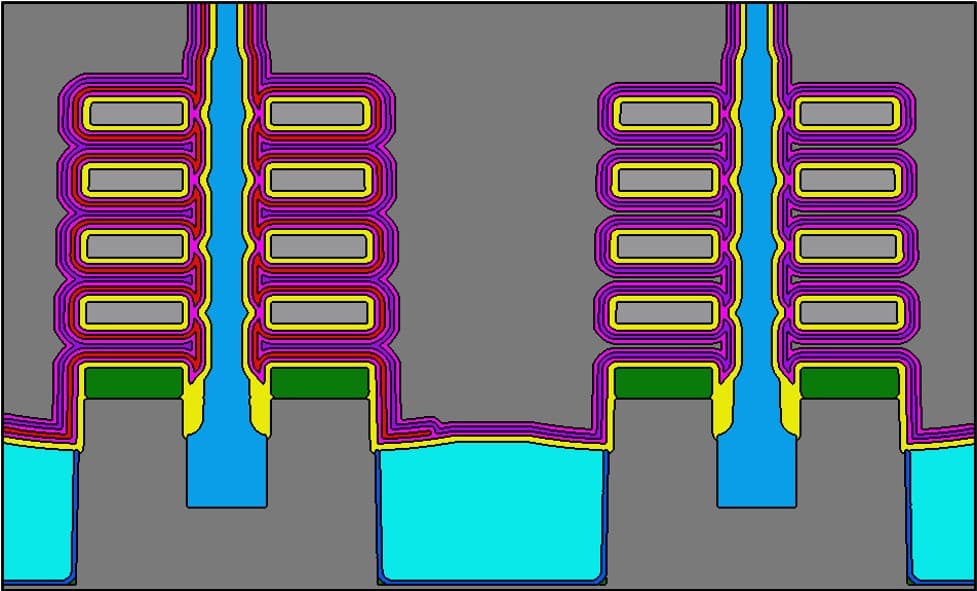
Illustration of the iN7 SAQP process.
In a next step, block features are added on top of the SAQP pattern. First, spin-on carbon (SoC) is coated on top of the spacer pattern. After resist coating, EUV exposure on the ASML NXE:3300 scanner then creates the block features in the resist material on top of the SoC. After SoC etch, pillar-like SoC block features of 65nm height stand on the spacer lines. This joint SAQP + block pattern is then patterned into the underlying TiN layer, which serves as a hard mask. By etching the trenches within this pattern into the low-k dielectric layer below, and metallizing them, the final metal2 pattern is obtained. The width of the block features determines the metal2 tip-to-tip critical dimension.
Assessing pattern fidelity and local variability
An important part of this work is to qualify the pattern fidelity and variability, as this will contribute to the viability of the proposed solutions for industrial manufacturing. At this small pitch of 32nm, even minor process variations in EUV lithography may have significant impact on the device performance. Such variations are due to overlay and CD uniformity, but also to stochastic effects in the resist.
In particular, the uniformity of the width and length of the block features are important parameters. The width of a block at the location of a trench determines the resulting metal tip-to-tip on that trench. The final target for the iN7 design is to achieve a critical dimension of 21nm metal tip-to-tip after low-k etch. The experiments show that the critical dimension is sufficiently uniform over the wafer. With further fine-tuning, it is expected to remain below 1nm 3sigma. Also the local variation of the block width and placement are important and determine the overlap of the metal line-end with the via that connects to a layer above or below. The major contributor to the local variation turns out to be the stochastic noise, coming from statistical variations in how the available photons interact with the resist. Added to the overlay (which involves the ability of the scanner to align the various layers accurately on top of each other), an edge placement error of the metal tip position of ~5nm 3sigma is obtained. Whether this provides sufficient overlap with the via layer, will depend on the design rule. For example, if no direct neighboring vias are allowed, there will be sufficient margin through the design extension of the metal tip over the via.
Another critical dimension is related to the length of the block, as this will be critical in determining the metal trench ‘blocking’ efficiency. A too short block feature could lead to an incomplete cut of the metal trench, and a too long feature can pinch neighboring metal trenches. Ideally, the block end is positioned halfway the spacer line. The maximum budget for the variation of the block end vs. the spacer edges is +/- 8nm. The dominant consumers of this budget are again the overlay and stochastics, adding to a local variation of ~6nm 3sigma. Thus, with a 3sigma requirement and if other contributors (such as intra-wafer CDU) can be kept small, the spacer width (16nm) is expected to provide sufficient budget to enable the SAQP + block technology for the iN7 node. Exact specifications may vary depending on the company and product.
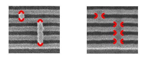
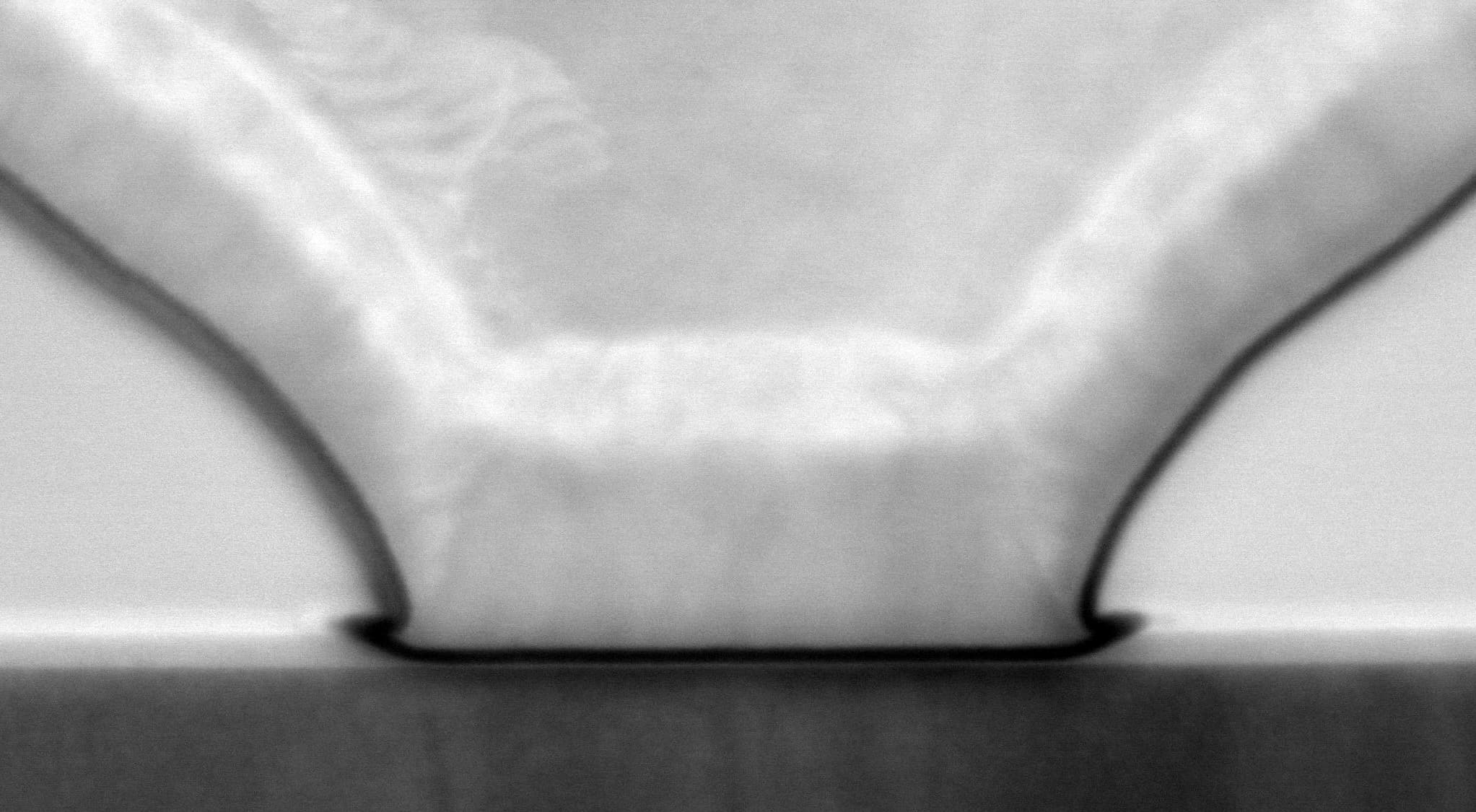
(Left) the length of the blocks determines the metal trench ‘blocking’ efficiency, while (right) the width determines the metal tip-to-tip.
Towards EUV implementation for high-volume manufacturing
Imec researchers have investigated the use of SAQP in combination with a single EUV blocking step for printing the critical 32nm pitch metal2 layer in the back-end-of-line. An important finding is that the current imaging performance of the ASML NXE:3300 is sufficient to print the metal2 block layer. The results clearly show the successful integration capability of the EUVL defined block. However, overlay and stochastics came forward as key attention points and will need further improvement, especially if further downscaling is pursued.
The proposed solution is a viable alternative to SAQP + immersion triple block patterning of the 32nm metal layer. From a cost perspective, a 20% cost reduction can be expected from the ‘hybrid’ solution with direct EUV block print, and EUV print of the vias. An additional cost reduction of 3% is expected from a scenario that uses only EUV in one single exposure for patterning the BEOL metal layers. First results point towards pattern fidelity and mask making as the main challenges for this option. Optimizations for this option are ongoing.
As pitch-only scaling doesn’t meet the full requirements for the foundry N5 node, the solutions have been complemented by co-optimizing the technology and the standard cell libraries, resulting in significantly lower standard cell heights. This will allow a full node definition whereby the wafer cost increase of scaling boosters (approx. 3%) is offset by an area reduction gain of approx. 21%.
Including the proposals for design rules, masks, photoresists, etching and metrology, for which imec worked in close collaboration with equipment and material suppliers, all these studies form the first comprehensive solution towards EUVL enablement for high-volume manufacturing.
Published on:
5 March 2017

