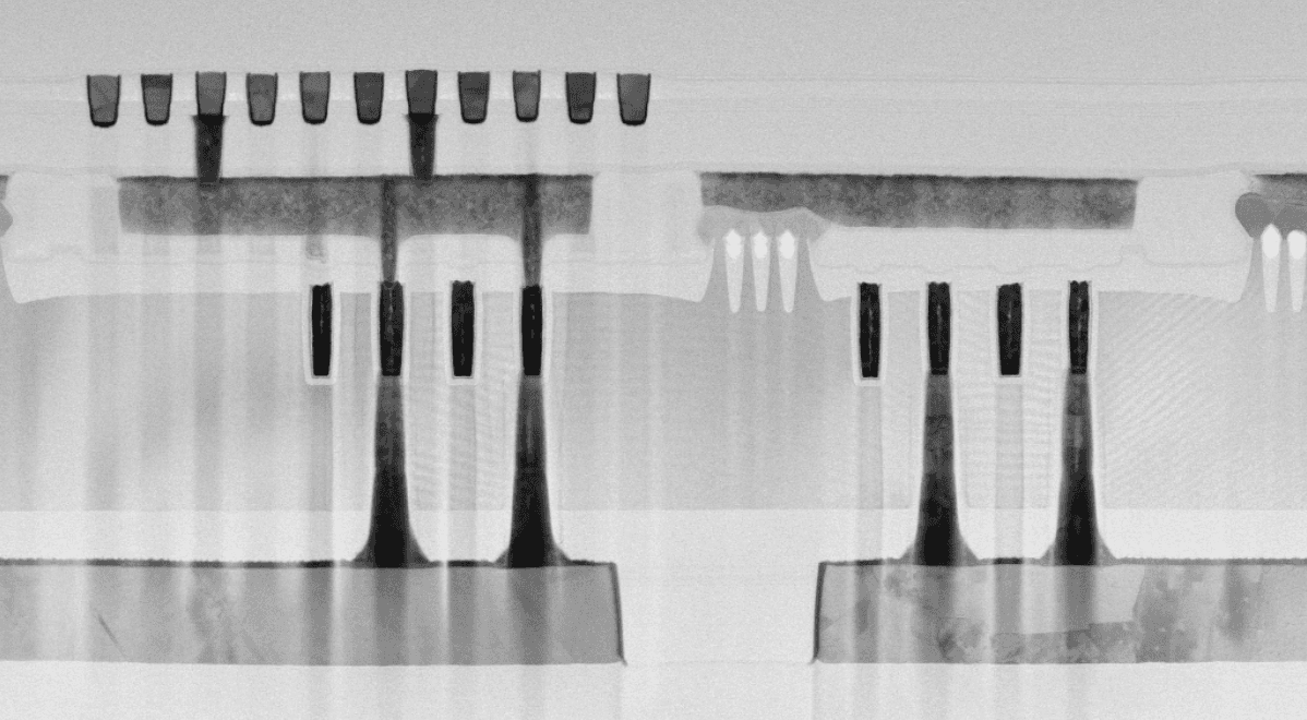
The promise of semi-damascene for future interconnects
In 1997, the introduction of Cu dual-damascene integration schemes in the back-end-of-line (BEOL) of logic and memory chips marked an inflection point in semiconductor history. Chip makers moved away from subtractive Al patterning to wet processes like Cu electroplating and chemical mechanical polishing (CMP). This radical transition was needed to cope with an increasing RC delay in Al-based interconnects, the result of an increasing resistance-capacitance (RC) product. Being cost-effective and applicable to multiple layers of the BEOL stack, Cu dual-damascene was set to enable many subsequent generations of logic and memory technologies.
But in a few years from now, the metal pitches within the most critical BEOL layers will drop below 20nm. When that happens, Cu dual-damascene, in turn, will run out of steam. As shrinking metal line dimensions approach Cu’s electron mean free path, the RC delay will increase dramatically. In addition, Cu metallization requires a barrier, a liner and a cap layer to ensure good reliability and prevent Cu from out-diffusing into the dielectric. But these extra layers start to consume a large share of the total available line width, meaning that the precious conductive area cannot be fully utilized by the interconnect metal itself. These issues force the chip industry to investigate alternative metallization schemes with better figures of merit at tight metal pitches.
After filing an initial patent in 2017, imec presented a new metallization concept to the semiconductor community in 2020 and named it ‘semi-damascene’ [1]. Just like the Al-based metallization, semi-damascene integration starts with the direct patterning (or subtractive metallization) of the first local interconnect metal layer, hence requiring a patternable metal such as W, Mo, Ru, etc. The via that connects with the next interconnect layer is then patterned in a single-damascene fashion: a hole etched into the dielectric is filled with metal and overfilled – meaning that the metal deposition continues until a layer of metal is formed over the dielectric. This metal is layer is subsequently masked and etched to form the second interconnect layer, with lines orthogonal to the first layer.
Do you want regular updates on imec’s semiconductor research?
Figure 1 – Schematic representation of imec’s semi-damascene flow: a) Ru etch (formation of the bottom local interconnect line (Mx)); b) dielectric gap fill or airgap formation; c) via etch; and d) via fill and top line (Mx+1) formation (pink = Ru; blue = low-k dielectric; green = hard mask).
The value proposition of semi-damascene is promising. It can be regarded as a two-layer metallization module potentially expandable to multiple layers – making it cost effective. The subtractive etch allows for higher metal line aspect ratios (ARs) than conventional Cu interconnects, improving the resistance. As for the dielectric, the metal lines can potentially be combined with airgaps instead of low-k dielectric gap fill. Airgaps offer a lower dielectric constant, leading to smaller intra-level capacitance. Besides being RC efficient, semi-damascene also eliminates the use of metal CMP, simplifying the process flow and resulting in improved line height control. The use of refractory metals also presents benefits. They have the promise to be used without barrier layer, hence providing low via and line resistance. They are also more resistant to electromigration and overall offer lower resistance than Cu at reduced dimensions.
The industry’s response: a promising but disruptive technology
Since imec introduced semi-damascene integration, multiple organizations started to research similar new schemes, and steady progress has been made through simulations and experiments [2-5]. Today, the very first step of the scheme, i.e., the subtractive etch of the first metal layer, has been successfully demonstrated and reported at conferences by multiple organizations. Experiments have clearly shown that replacing Cu with subtractively etched Ru in the first local interconnect layer can already provide a much-wanted benefit, even at a modest line AR ~2. For subsequent generations the AR can be increased to 3 or 6 and then combined into multiple local metal layers. R&D evidence is growing that semi-damascene is indeed a valid option, offering an interconnect scaling path.
At the same time, there are question marks. Industry is currently considering moving the first generation of semi-damascene into development, the phase before actual production. As with any new technology, industry does not proceed overnight. Semi-damascene integration disrupts the conventional technology for fabricating the BEOL. It requires new tools and materials, and perhaps some of the defect mechanisms are not captured in the research phase. Such investments are of interest only if the technology can span several technology generations. While the first step with only one metal layer is adequately documented, the implementation of a two-layer and even multi-layer integration scheme – where the capabilities and benefits of semi-damascene can be fully exploited – is however less discussed. That’s why imec encourages the R&D community to open the discussion, help filling the remaining ‘gaps’ and share insights on multilayer integration at interconnect technology conferences.
The imec interconnect roadmap: introducing 5 generations of semi-damascene
Imec proposes to gradually introduce subsequent generations of semi-damascene. Insertion of the first generation is envisioned for the imec A10 or A7 logic technology node, where the metal pitch of the most critical interconnects becomes as tight as 18nm. At that point in time, GAA nanosheet integration is expected to be mainstream and CFETs will not yet be in place. Introducing semi-damascene will therefore be the only major change that chip makers will have to cope with.
Figure 2 – The imec logic roadmap.
Imec proposes to introduce subtractively etched Ru in M0, the first local metal layer that follows the middle of line (MOL). This first generation will come with a metal line AR 2, which is slightly higher than today’s typical Cu line AR (~1.6). In combination with the favorable behavior of barrier-less Ru at tight metal pitches, this approach will already give a resistance and reliability benefit over Cu.
In the second generation, imec aims to increase the AR of the M0 interconnect line to 3, which will further lower the resistance, and combine the M0 with a barrierless via. As higher ARs tend to increase the intra-level capacitance, this generation needs airgaps instead of low-k dielectric gap fill. Besides offering a lower dielectric constant, working with airgaps also avoids the ‘gap fill issue’: the challenge of filling narrow trenches with dielectrics in a uniform way.
By adding a via and a second metal layer in semi-damascene fashion, generation three will see true semi-damascene integration of both the M0 and M2 local metal layers – the most critical layers of the BEOL. The fourth generation may see even more layers of semi-damascene. The AR will be gradually ramped up to 4, 5 and even more – depending on what will be feasible. Up to ~AR=6, when combined with airgap, sufficient RC benefit over other options is expected.
On the longer term, call it generation five, imec envisions alternative metals to enter the semi-damascene roadmap. Think about patternable binary or ternary compounds with better figures of merit than single metals at tight interconnect pitches.
Figure 3 – The imec semi-damascene roadmap, introducing subsequent generations of semi-damascene with improved RC (HM = hard mask; DD = dual-damascene; SD = semi-damascene).
As such, semi-damascene can become the next inflection point for BEOL fabrication. It has an excellent value proposition, not only in terms of resistance, capacitance, and area consumption. Experiments and simulations also point towards lower power consumption and better thermal properties than Cu dual-damascene schemes. At the same time, the stepwise implementation as outlined above will allow to minimize the risks always associated with the introduction of a new technology.
Enabling advanced generations of semi-damascene
While generation one and two are ready to enter the development phase, more research is needed to demonstrate and mature the next generations of semi-damascene. The main challenges can be grouped around multi-layer semi-damascene integration, increase of the AR, and exploration of new metals for generation five.
Below is a grasp of recent progress reported by imec researchers. The results are not only meant to fill in the remaining gaps. They also aim to trigger the discussion and encourage other research institutions to complement imec’s research – to the benefit of the entire ecosystem.
Towards multi-layer integration schemes in advanced interconnect
As already mentioned, semi-damascene is in essence a two-metal-layer integration scheme, potentially expandable to multiple layers. But process optimizations for multilayer schemes are still in their infancy. What is the best way to implement them? Which litho and etch processes, hard masks and resists should be used? And how to integrate the vias that connect the extremely narrow interconnect lines of subsequent BEOL layers?
To address the last question, imec earlier proposed the fully self-aligned via (FSAV) as a key building block to semi-damascene [6]. FSAVs ensure a proper alignment of the lines and via (at both via top and bottom), which is crucial to enable low via-to-line leakage. So far, several integration schemes for the FSAV have been presented by multiple research organizations, including imec.
At IITC 2024, imec was the first to benchmark different FSAV integration options, aiming to explore how the FSAV can be best implemented in the 300mm fab [7]. In other words: how can we meet the target via resistance with optimal via-to-line overlay, and at the same time ensure low variability and good reproducibility across the 300mm wafer?
Besides the conventional single-damascene scheme (FSAV) to create the via (meaning that the via is created by etching a hole in a SiO2 dielectric which is then filled with metal), imec explored two pillar-based FSAV integration schemes (meaning that the via is formed as a pillar by direct etch of a metal layer). The two variants are referred to as ‘hybrid pillar’ (HP-FSAV) and ‘pillar with an etch stop layer’ (PE-FSAV).
Figure 4 – Via resistance distribution and cross-sectional TEMs for the three different FSAV options at 26nm metal pitch.
The three integration schemes differ in number of process steps, and in patterning and etch processes being used, in hard mask integration and type of resist (e.g., allowing EUV lithography tone inversion for enabling the pillars). But for all three cases, the feasibility of reaching target via resistance and via-to-line overlay margin was showcased. The most notable difference is related to the resistance uniformity achieved across the wafer. All integration schemes provide sufficient via litho and etch process windows. Therefore, they are compatible with the direct metal etching equipment currently available through our tool suppliers. Other work by imec shows that the self-aligned window also exists for implementing airgaps, which will be needed to continue the capacitance benefit when line ARs increase further [8].
Figure 5 – Via resistance distribution for overlay across the MX line, showing overlay margin. In the 3D cartoons, an overlay shift of ~7nm is shown for the three FSAV options
The status today hence proves that technically viable options are available to implement at least two layers of semi-damascene. At the same time the number of wafers demonstrated is limited. Hence, imec encourages other organizations to complement the puzzle, and let the industry ecosystem ‘decide’ on the best option forward.
Incrementally increasing the aspect ratio of semi-damascene lines: understanding and mitigating the roadblocks
A continued decrease of the resistance of Ru semi-damascene lines is possible by further increasing their AR. In 2022, imec showed first evidence that implementing semi-damascene with AR 6 can indeed substantially improve the RC metric over lower AR schemes [9]. Shortly after, initial experiments indicated that high-AR lines are also compatible with multilayer schemes [10].
While the formation of interconnect lines with modest ARs (2 and 3) is relatively well understood, increasing the AR while preserving good line resistance and reliability requires some technical mastery. It has shown to challenge almost every process step – including patterning and etch, cleaning, and defect control. For example, the direct metal etch ‘attacks’ the sidewalls of the Ru lines, leading to line-break defects. And this worsens with increasing AR. Obtaining the lowest possible line resistance necessitates a more fundamental understanding of the high-AR line formation and reliability.
Figure 6 - Towards higher AR metal lines.
As a first important insight, researchers at imec found that the composition of the stack used to form the high-AR metal lines strongly influences the resistance of the semi-damascene lines. Line break defectivity was shown to be the main contributor to the stack-dependent device performance. Imec, through multiple experiments, found an optimal stack, which starts with depositing 1nm TiN for improved adhesion, followed by physical vapor deposited (PVD) Ru. Compared to other compositions used in the study, this stack offered the lowest resistance over the entire height of the metal line. Second, the study provided a first indication that the line defectivity is influenced by the grain structure and crystal orientation of the Ru metal grains. These morphological parameters strongly depend on the method used for depositing Ru, favoring the use of PVD. [11]
Besides gaining insights in the parameters affecting the Ru line resistance, imec recently came up with a unique approach to further improve the high-AR lines from resistance and uniformity point of view: sandwiching a sub-nm TiN or W layer between two Ru layers. This stack was found to be less prone to lateral attack and line-break formation during direct metal etch compared to stacks without this extra layer. The key benefit of this ‘defect mitigation layer’ is that it enables low-defectivity lines of high AR and long lengths, which is a promising result towards AR≥6 Ru semi-damascene. The results were presented at the 2024 VLSI Symposium [12]. The experimental work showed good reliability behavior of lines down to 24nm pitch. But, at the same time more work is needed to optimize and extend the results towards 18nm pitch, show compatibility with integrating airgaps and demonstrate sufficient time-dependent dielectric breakdown (TDDB) and mechanical reliability margin.
Figure 7 – Resistance yield of AR 6 lines at various metal pitches (18-26nm) for cases with and without defect mitigation layer (DML).
Advanced interconnects: the quest for alternative conductors
The work on semi-damascene integration so far focused on using Ru as the conductor of choice. Several years ago, imec began investigating whether there are other metals with even better prospects. The search expanded from elemental metals towards binary and ternary ordered compounds [13]. After a promising preliminary study, several R&D groups worldwide started to embrace the idea and joined the search for candidate alloys. The community recently gathered at the VLSI 2024 thematic workshop on ‘Novel metals for advanced interconnects’. This workshop was organized by imec to discuss the state of the art and future research directions – from both industrial and academic perspective.
Since the list of potential alloys is enormous, imec started its investigation with setting up a unique methodology for down-selecting and ranking the possible candidates. Two figures of merit were identified for benchmarking against Cu: the compound’s cohesive energy and the product of the bulk resistivity and the mean free path of the carriers. Ab-initio simulations revealed a sub-list of candidates, including for example intermetallic aluminides, the starting point for further experimental work.
Today, research groups worldwide investigate how the resistivity of these candidate alloys behaves at reduced dimensions. For example, when intermetallic aluminides are deposited in thin films, defect mechanisms involved in thin film formation seem to affect the resistivity behavior. Understanding that correlation will be key to control the resistance. Imec also identified global and local composition control as an important knob towards minimizing the resistance. [14]
Figure 8 – Example of the challenge posed by local composition control in intermetallic aluminides. The atom probe tomography measurement (right) shows local composition fluctuations (blue = Al; green = Ni), affecting the resistivity (left).
Once ways are found to optimize the resistance of promising binary and ternary alloys, the next step is to implement them in relevant metallization schemes and address the challenges related to semi-damascene processing. Imec encourages universities and research groups to collaboratively explore patterning and etch strategies and set up process directions. Although much work remains to be done, research into alternative metals is a promising avenue, and steady progress is being made. Intense collaborations will yet be needed to eventually introduce them into generation five of semi-damascene integration.
Conclusion
Semi-damascene metallization may become the next inflection point in BEOL fabrication, with industry currently debating about introducing subtractive etch in the first local interconnect layer. Although not even the first generation of semi-damascene is in production today, based on experimental evidence, imec is already looking ahead to newer generations of semi-damascene. The focus is on multiple metal layers and vias, a step-by-step increase of the aspect ratios, and the introduction of new metals. For these next generations to become a reality, joint efforts and more data are needed with strong input from academia and industry.
This article was originally published in Semiconductor Digest (pgs 28-33).
Want to know more?
[1] ‘Semidamascene interconnects for 2nm node and beyond,’ G. Murdoch et al., IEEE IITC 2020;
[2] ‘Subtractive Ru Interconnect Enabled by Novel Patterning Solution for EUV Double Patterning and Top Via with Embedded Airgap Integration for Post Cu Interconnect Scaling,’ C. Penny et al., IEDM 2022;
[3] ‘Airgap Integration on Patterned Metal Lines for Advanced Interconnect Performance Scaling,’ H.K. Chang et al., IEEE IITC 2023;
[4] ‘A Novel Integration Scheme for Self-Aligned Ru Top via as Post-Cu Alternative Metal Interconnects,’ K. Motoyama et al., IEEE IITC 2023;
[5] ‘A Study of Resistivity Control for Subtractive Interconnects Using Ruthenium,’ J. Rogers et al., IEEE IITC 2023;
[6] ‘First demonstration of two metal level semi-damascene interconnects with fully self-aligned vias at 18MP,’ G. Murdoch et al., VLSI 2022;
[7] ‘Redefining 2-level semi-damascene interconnect technology: benchmarking three different fully self-aligned via options,’ G. Marti et al., IEEE IITC 2024;
[8] ‘Airgap integration in MP18 two-level semi-damascene interconnects with fully self-aligned vias,’ G. Delie et al., IEEE IITC 2024;
[9] ‘MP18-26 Ru direct-etch integration development with leakage improvement and increased aspect ratio,’ A. Pokhrel et al., IEEE IITC 2022;
[10] ‘Two-metal-level semi-damascene interconnect at metal pitch 18nm and aspect-ratio 6 routed using fully self-aligned via,’ A. Gupta et al., IEDM 2023;
[11] ‘Impact of Ru deposition method and adhesion layer on electrical performance of semi-damascene interconnects,’ G. Delie et al., SSDM 2023;
[12] ‘Mitigating line-break defectivity with a sandwiched TiN or W layer for metal pitch 18nm aspect ratio 6 semi-damascene interconnects,’ A. Gupta et al., VLSI 2024;
[13] ‘Alternative metals: from ab initio screening to calibrated narrow line model’, C. Adelmann et al., IEEE IITC 2018;
[14] ‘Optimizations on resistivity of binary compounds for advanced interconnect metallization,’ J.-P. Soulié, SSDM 2023.

Zsolt Tokei is imec fellow, program director nano-interconnects at imec. He joined imec in 1999 and since then held various technical positions in the organization. First as a process engineer and researcher in the field of copper low-k interconnects, then he headed the metal section. Later he became principal scientist, and program director nano-interconnects. He earned a M.S. (1994) in physics from the University Kossuth in Debrecen, Hungary. In the framework of a co-directed thesis between the Hungarian University Kossuth and the French University Aix Marseille-III, he obtained his PhD (1997) in physics and materials science. In 1998 he started working at the Max-Planck Institute of Düsseldorf, Germany, as a post-doctorate researcher. Joining imec, he continued working on a range of interconnect issues including scaling, metallization, electrical characterization, module integration, reliability and system aspects.
Published on:
31 October 2024
