The need for bottom-up life-cycle assessment
Lars-Åke Ragnarsson: “In response to rising concerns about climate change, tech companies around the world are accelerating their efforts to achieve carbon neutrality for their supply chains and products. In this, the semiconductor industry has a major role to play.
Studies have found, for example, that more than 70% of the carbon footprint generated over the lifetime of a smartphone can be traced back to the manufacturing process, with nearly half of that share, or around 40% of the total, coming from chip production.
To reduce the environmental impact of chip manufacturing, we must understand how large the impact is, what parts of the manufacturing have the largest impact, how it will evolve towards the future and what levers we have to reduce it.
But life cycle inventory databases that are available today lack the data needed to complete such analysis. For example, they do not cover advanced technologies like 3D NAND and logic technologies beyond 14 nm.
Furthermore, most companies take a top-down view: they basically look at the yearly production of their fab, and look from procurement at how much electricity, how much water, and how much of the other resources have been consumed.
What’s missing is a higher granularity of results – process- and fab-level insights, for example. Such a bottom-up view would allow us to identify high-impact areas and make projections for the future.
Closing the data gap necessitates a holistic approach and sharing emissions data across the entire manufacturing lifecycle and supply chain. I would therefore call on the semiconductor industry for as much transparency as possible, and for pursuing a high degree of uniformity in sustainability-data collection and reporting – following the standards as proposed by SEMI’s Semiconductor Climate Consortium (SCC).”
Assess, improve, disrupt
“In 2021, imec launched its Sustainable Semiconductor Technologies & Systems (SSTS) program to help the IC manufacturing value chain reach its environmental sustainability targets. The program is structured around three pillars: assess, improve, and disrupt.
At the heart of the ‘assess’ pillar lies our in-house developed software platform, called imec.netzero. It functions as a virtual fab which gives a quantified bottom-up view of IC manufacturing for current and future logic and memory technologies.
Imec.netzero aims to become the industry standard to estimate energy consumption, water usage, mineral usage, and greenhouse gas emissions associated with the different processes involved in chip fabrication. Unlike other models, it provides actionable data down to the process step and processing tool level, allowing projections for future technologies and identification of high-impact processes.
For these high-impact processes, collaborative projects are being conducted within the ‘improve’ pillar, where we explore solutions to minimize their impact in our partner’s facilities or using imec’s 300mm fab as a pilot environment.
The long-term aim – pursued in the ‘disrupt’ pillar – is to develop an environmental impact toolbox with E metrics and protocols. This will ultimately enable green technology pathfinding through Power-Performance-Area-Cost-Environment (PPAC-E) analysis of new IC technologies.
Learnings from the program will be used to publish guidelines for program stakeholders, and to engage with Semi SCC for setting up a roadmap to help achieve net-zero in the industry. High-level learnings and data will also be shared with the scientific community and broader public.
In November 2023, we released a public version of our imec.netzero web application to the broader public, providing them with a tool to obtain high-level information about the environmental impact of chip manufacturing.
Going beyond what exists today, such a tool can be valuable to designers who need to make life cycle assessments of their products, to academics who study the environmental impact of ICT and to policy makers who need information about the impact from industry.
To our SSTS program partners, we offer a more comprehensive version of the imec.netzero tool. The partner version exploits the same fab models and process databases as its public variant, but it releases more details, allows to identify high-impact areas, models future technologies and gives more options to parameterize the virtual fab models. It allows our partners to be at the forefront of one of the most important innovation domains in our industry and gives them a head start in green technology pathfinding.”
A key role for industrial players
“The success of our approach hinges on the active involvement of players from across the entire IC value chain. We are therefore very pleased to have several renowned system and fabless companies, equipment, infrastructure, and material suppliers, as well as IDMs and foundries as partners in our program.
IDMs and foundries, for example, can help us benchmark the numbers. We build models from the bottom up, based on data collected from different sources, including imec’s fab. But there are always some parts that we miss. Foundries, on the other hand, have the top-down view. They can bring our models closer to reality and help us further refine and optimize our imec.netzero tool.
All program members gain access to a unique ecosystem of partners. They discuss, for example, how to set up a roadmap to achieve net-zero with the entire supply chain on board.”
First results: LCA analysis of logic nodes; importance of gas abatement; hydrogen recovery; reducing F-gas emissions
“As part of the assess pillar, we are continually optimizing our virtual fab model by enriching the data and benchmarking the results. Our model is based on bottom-up life cycle assessment (LCA) of a generic high-volume manufacturing fab. At the 2023 IEDM conference, we presented an LCA analysis of logic technology nodes (N28 to A14) and benchmarked our work with other LCA databases [1].
When evaluating the total emissions in terms of their global warming potential (GWP), our estimates are observed to be slightly lower than others. This is not very surprising since we are still building our inventory, and our data will be further refined in the coming months. Furthermore, the scope and methodologies of the different studies differ somewhat, making one-to-one comparison difficult.
In our studies, we show a detailed breakdown analysis of the total emissions. We highlight, for example, the importance of deploying efficient process gas abatement, as it can have a high impact on reducing total greenhouse gas emissions.
Do you want regular updates on imec’s semiconductor research?
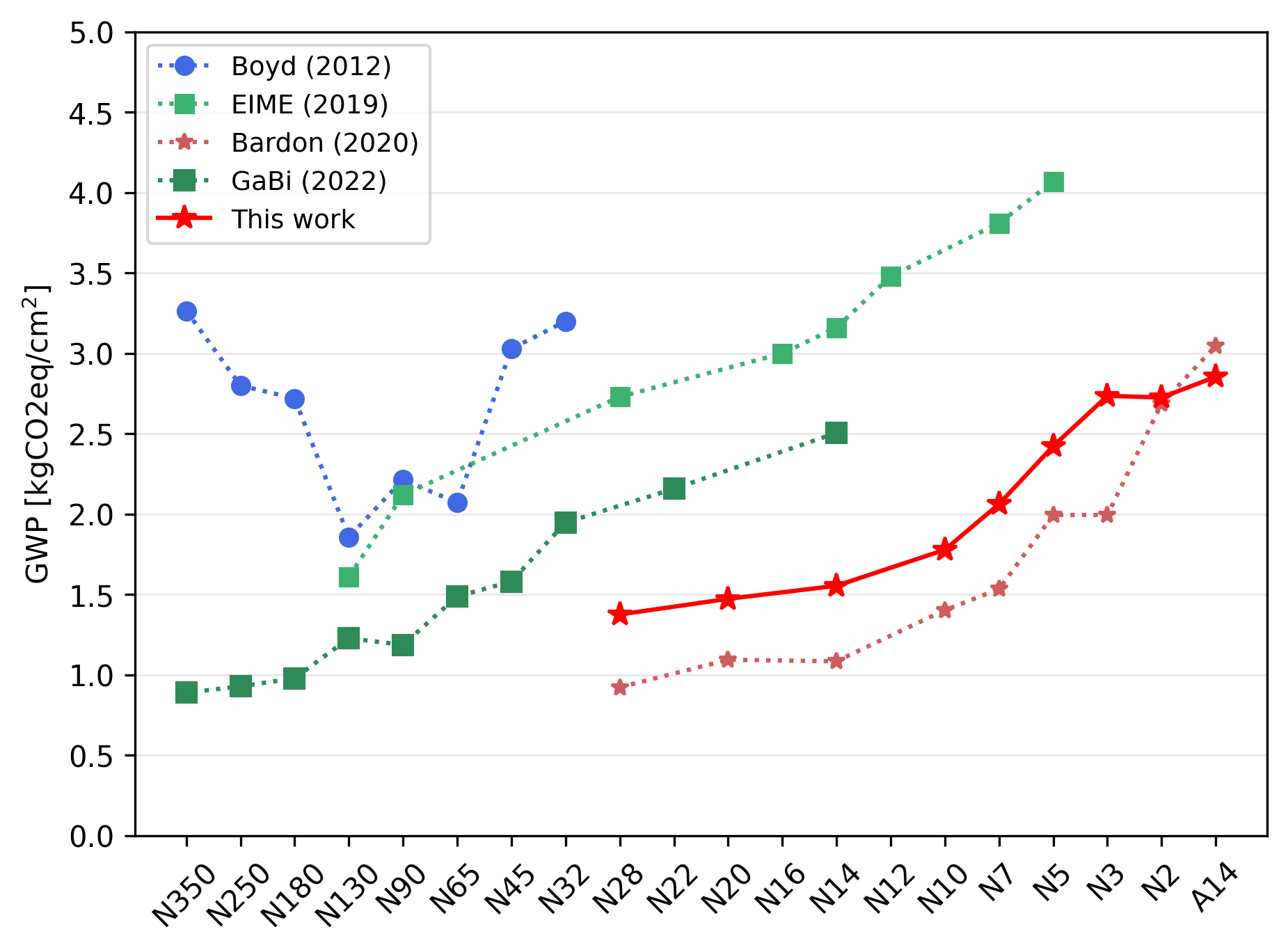
Benchmarking of imec’s SSTS assess work with other LCA databases and scientific literature values (as presented at IEDM 2023).
Within the SSTS improve project, we work out solutions for four focus areas: energy efficiency, greenhouse gas emissions, water management, and material circularity. In collaboration with our partner Edwards, imec already installed a hydrogen recovery system for extreme ultraviolet (EUV) lithography in our 300mm cleanroom, enabling us to reuse and recover about 70% of the hydrogen.
In another project, we focus on reducing fluorinated gas emissions in etch processes – which takes a large share in the total greenhouse gas emissions. We not only focus on finding alternatives for these F-gases, but take a holistic view to etch, for example, by optimizing the stack of material layers used for the etch process. Initial results show that etch process and stack optimization improve the emissions by over 60%.”
Towards green technology pathfinding
“Developing new technologies for e.g., logic and memory was so far synonymous with resolving the PPAC (Power Performance Area Cost) trade-off. With cost as a main driver, environmental aspects were sort of an ‘afterthought’. Only when environmental considerations increase the cost of a certain technology – think about rising carbon taxes, or scarce raw materials becoming too expensive – will the semiconductor industry start to look for more environmentally friendly alternatives.
To enable true sustainable development, however, the environmental impact needs to be taken into account in the very early stages of technology pathfinding – by adding ‘E’ to PPAC. This is what we are pursuing within the disrupt pillar of the SSTS program
Solving the PPAC-E trade-off for new technologies is not only complex, but it also requires a new mindset. It has taken us years to find the right materials and to refine the process modules and steps that have contributed to the progress of the semiconductor industry. So, in addition, none of the alternatives may compromise the performance of the existing tools and processes, and ultimately of the devices.
This may seem like a daunting task. But we are confident that, by joining forces, we can do it. After all, there is too much at stake.”
Outlook: expanding the technology portfolio; reducing PFAS
“Within the assess pillar, we continue to improve and expand our life cycle inventory. So far, we included logic technologies – current and future nodes – and DRAM and NAND Flash memory technologies. We recently started adding packaging technologies and advanced RF technologies to our portfolio.
In the next three years, we will gradually expand our life cycle inventory with more system-level technologies like 3D integration. In parallel, we are building a system application, allowing to gradually combine the various technologies into a system package. This will enable our partners to assess the environmental impact of manufacturing full-system solutions.
We are however aware that not all environmental impact is captured in the carbon (equivalent) emission metric. For example, many of the materials used in IC manufacturing contain PFAS (per- and polyfluoroalkyl substances). The bioaccumulation potential of these substances has led to a strong societal interest in eliminating their use.
Eliminating PFAS is a complex task since it is embedded in many of the IC processing steps. It is present in, for example, chemically amplified resists for optical lithography, it is a critical component of most cooling liquids, and it is contained in several of the F-gases for cleaning and etch.
Under the form of Teflon, PFAS is also omnipresent in processing and cleaning equipment – think of O-rings and other sealing products. We are setting up plans to support our equipment and material suppliers with the reduction of PFAS as much as possible, in addition to our projects that lower carbon emissions directly.”
This article was originally published in Nature Reviews Electrical Engineering.
Want to know more?
[1] ‘Cradle-to-gate life cycle assessment of CMOS logic technologies’, L. Boakes et al., 2023 IEDM
Interested in receiving this article? Fill in our contact form.
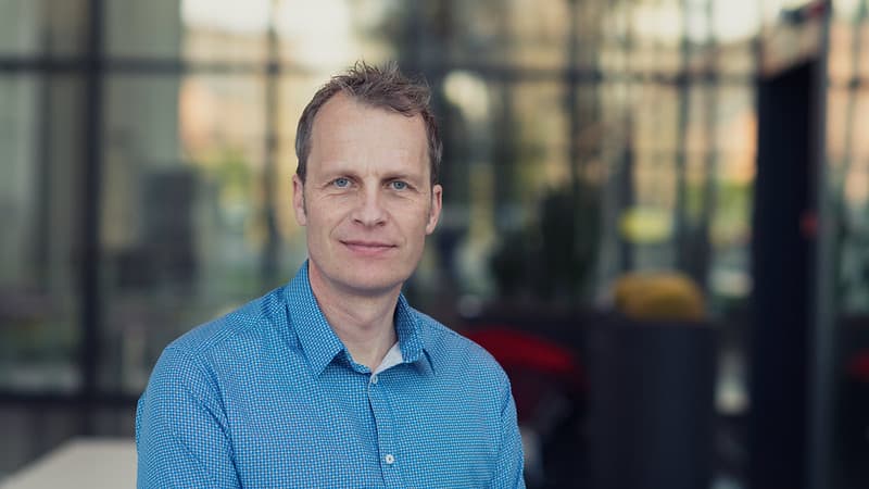
Lars-Åke Ragnarsson is program director of sustainable semiconductor technologies and systems (SSTS) at imec. He received his M.S. and Ph.D. degrees in electrical engineering from the Chalmers University of Technology in Göteborg, Sweden. From 2000-2002, he did postdoctoral studies with the IBM T.J. Watson Research Center in Yorktown Heights, NY, focusing mainly on the electrical characterization of high-k dielectrics. Since 2002, he has been with imec, focusing on developing advanced technologies using high-κ dielectrics and metal gates. Today, Lars-Åke is program director in compute and memory technologies, focusing on the sustainability of current and future technologies.
Published on:
1 March 2024

