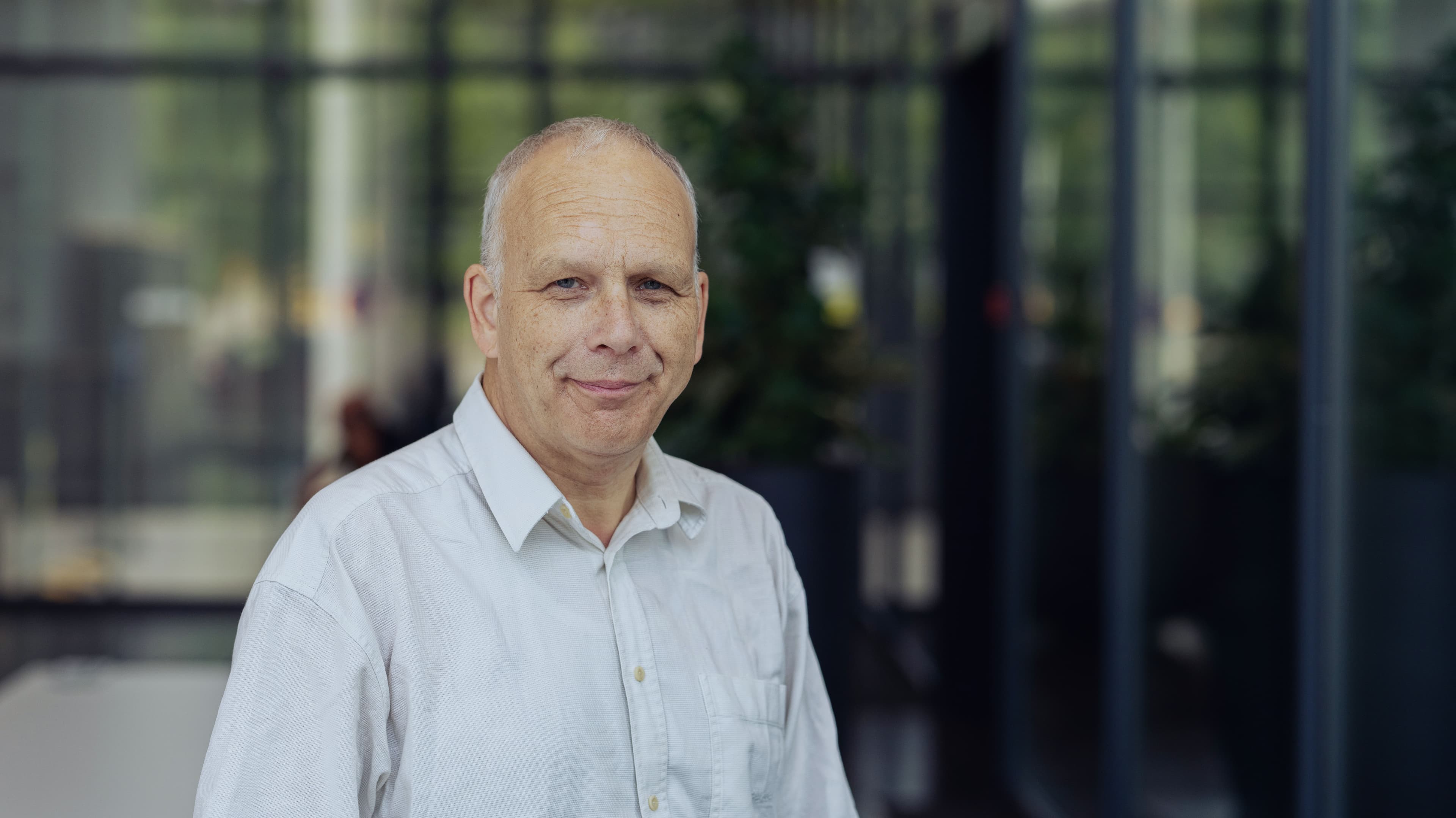
Who is Christian Haffner?
“I was born in the region of the Black Forest in Germany; in 1986, which is two years after imec was founded. Throughout my education, I have sought to balance the engineering side of physics and the physics side of engineering. This eventually led me to the area of applied physics and, more specifically, photonics and optics. Another important driver in my educational and professional career has been to ensure that groundbreaking insights happen and find their way into relevant applications. That’s why I always want to have one foot in fundamental and another in applied research.
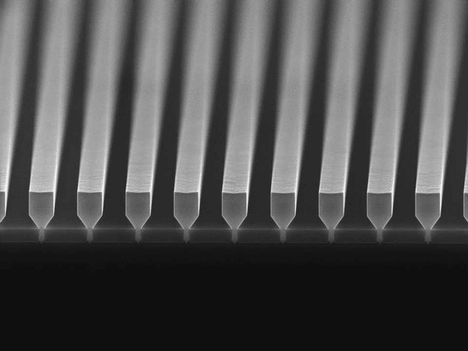
When I followed my Ph.D. supervisor in his transition from Karlsruhe Institute of Technology to ETH Zurich (Switzerland’s leading university for science and technology), I had the privilege of working in plasmonics after the initial hype. Plasmonics was a promising technology because it allowed electronic systems to communicate at extremely high speeds. Tremendous research efforts initially went into the field, and in terms of publications, the low-hanging fruit was already harvested as I entered the field. Our team tackled some of the main roadblocks this technology was facing, specifically in the physical layer for optical communication. The biggest downside of plasmonics was that the high speeds went hand in hand with high energy losses. Our team managed to develop various solutions to overcome these losses and published, as a first author, several papers in leading magazines such as Nature Photonics, Nature and Science. I am still very proud that we managed to do so at a time when it wasn’t trivial to get your work on plasmonics published. It also boosted me to pursue my academic career further. After my Ph.D. and postdoc at ETH, I joined the National Institute of Standards and Technology (NIST) in the U.S. During my two-year postdoc, I was pointed towards imec’s tenure track and decided to apply.”
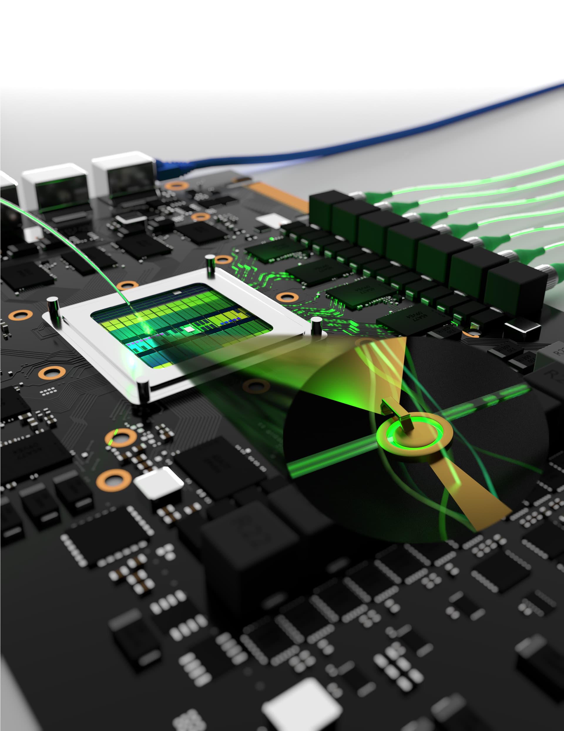
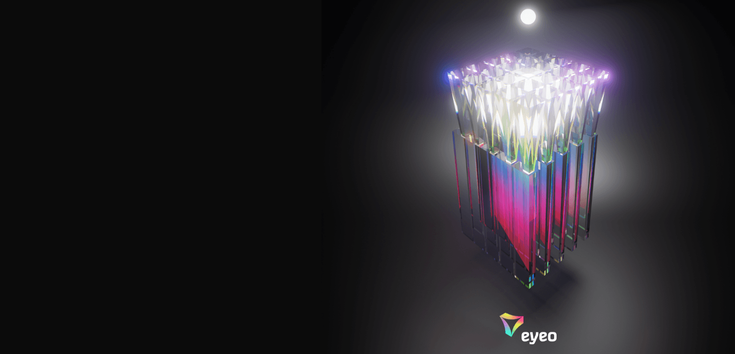
Artist impression of Christian Haffner’s Ph.D. work on plasmonics for optical communications. (Courtesy of Nathaniel Kinsey Virginia Commenwealth University)
And very successfully, as you came out first out of 88 candidates. How did you find out about imec’s tenure track, and how did you experience the selection procedure?
“It was my wife who saw an imec ad and sent it to me. I was a bit confused at first since I knew imec as a leading research organization but wasn’t immediately expecting them to have a tenure track. After I gave it a second look, I got increasingly enthusiastic about the offer. Firstly, it gave me a similar context as at NIST, namely to perform fundamental research without the requirement of teaching. Secondly, the package imec offers cannot be overestimated. Building your own team with two PhDs and a postdoc, the ability to equip your own lab, access all other state-of-the-art facilities, and getting a permanent contract seem like unique opportunities to me.
Throughout the entire selection and onboarding, I have experienced my application as a two-way dialogue. Although everything happened online – I signed the contract without ever having visited the imec premises – I felt an authentic connection with the imec people I was speaking with. The stepwise approach allowed me to go through the procedure without an unacceptable workload, and imec acted as a sparring partner to bring focus along the way. I also want to give imec much credit for its unbiased search for the right candidate. Apart from a reference letter from my supervisor, I did not have internal contacts, nor did I personally know anyone within imec.
In parallel to the imec tenure track, I am also a beneficiary of a Branco Weiss Fellowship for which I applied in 2019. It’s a support program and community for young scientists that bring science and society together. It’s a very flexible program, and it was my original motivator to move my research focus to the topic I am now working on: integrated electro-optical devices for quantum applications.”
What kind of quantum applications do you mean? And equally important: why do we need them?
“Starting with the last question, everyone knows by now that global energy demand is one of the fundamental challenges for which our society needs long-term solutions. While energy consumption is skyrocketing, the available energy resources will always remain limited. Data communication has become the fastest growing sector in the past two decades in terms of energy consumption. This should not come as a surprise if you think of entertainment and the enormous amounts of data streamed across the globe. Together with the entire semiconductor industry, it is, therefore, my ambition to help minimalize the energy cost per transmitted bit.
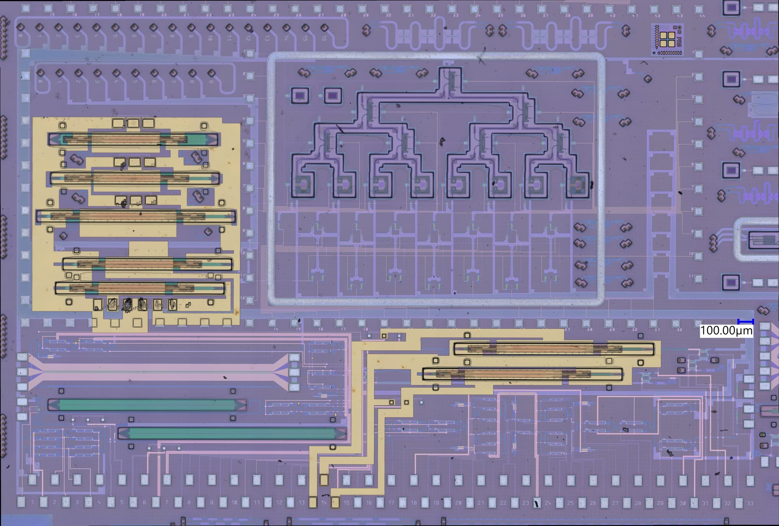
And that’s where the domain of photonics comes in. By using light (photons) instead of electricity (electrons), photonic systems can combine high bandwidths with little or no losses, resulting in energy-efficient systems. Photonics has taken over the backbone already, from the large data centers down to fiber to the home. One of the challenges now is to integrate photonics into the chip and board level. Because even within a CPU, around half of the energy is consumed by on-chip communication instead of computation. A number that is expected to grow to 80 percent if we extrapolate the latest trends. Integrated photonics can drastically reduce this on-chip communication energy but is not optimal to perform digital logic. Future systems will therefore use electronics for computation and photonics for communication. This reveals the need to have integrated switches that can convert light into electricity and vice versa. Or, in other words: electro-optical devices. Such technologies are already under development for the ‘classical’ domain of silicon photonics and are proving their value on the level of data centers and higher-level infrastructures. To help tackle the challenges on the chip level, we go a few steps further and look into them for quantum applications.”
What are these electro-optical devices, and why are they hard to develop?
“Letting optical signals talk to electrical signals is challenging as photons oscillate almost a million times faster than electrons. As one of the consequences, relatively high voltages are required to manipulate the photons. This is the main reason why creating opto-electronic switches poses considerable challenges in the domain of integrated Silicon photonics.
While research is moving forward and gradually coming up with solutions, we aim to provide an additional angle of approach by skipping some steps and immediately raising the bar even further. If these switches impose challenges for traditional information processing, they will likely do so for quantum computing as well. Looking at the literature, we see that existing quantum approaches rely on various kinds of qubits. Some are represented by what are called ‘RF photons,’ which have similar drawbacks as electrons in terms of long-distance communication and need to be cooled down to milliKelvin temperatures. It’s hard to imagine a milliKelvin communication line from London to New York. So the quantum domain is faced with similar challenges as the classical domain, only more complicated: how can we convert a single RF photon into a single light photon and back? We are talking about 10-12 orders of magnitude smaller signal energies than in classical photonics. This is like the ultimate boundary for electro-optics. And the beauty is that if we can make progress on this for the quantum domain, the classical integrated photonics will also benefit from our learnings. And that’s the motivation for the work that we are about to start within the tenure track.”
What’s the status of your activities, and what do you hope to achieve in the foreseeable future?
“I am relocating to Belgium as we speak and starting to get acquainted with the new work environment. Which, for obvious reasons, already poses some additional challenges in the current COVID-19 context. But overall, we are ramping up quite well. The two Ph.D. positions in our team are already filled in by strong candidates, and we hope to find an additional postdoc soon. For the lab, we have purchased our first dedicated piece of equipment, which will help us to do cryogenic electro-optical characterization. And, thanks to the good guidance by my new colleagues at imec, we have submitted a proposal to obtain a European Research Council (ERC) grant. I am quite confident that we will soon be able to perform some first experiments and get some additional preliminary data to verify that our ideas are the right ones. From that point onwards, our clear ambition is to do those things that no one else is doing. And where that will lead us, no one knows.”
Want to know more?
- More about imec’s tenure track (new application will open in September 2024): Imec - Tenure Track | imec (imec-int.com).
- Webpage for Christian Haffners’s Branco Weiss Fellowship: Fellow Details - The Branco Weiss Fellowship - Society in Science
- Article featured by the Optical Society on how the ETH team Christian Haffner was part of solved some of the plasmonics’ challenges related to energy loss: Taking Advantage of (Plasmonic) Loss | Optics & Photonics News (osa-opn.org).
- Article in IEEE Spectrum explaining more about integrated photonics and featuring Christian Haffner’s earlier breakthroughs in electro-optical systems: Photonics Meets Plasmonics in New Switch That Could Steer Lidar Laser Beams - IEEE Spectrum.

Christian Haffner was appointed to imec’s new tenure track program in March 2021, where he is building a research team to explore the limits of electro-optics. Before his appointment, he performed postdoctoral research exploring the limits of electro-optics at the National Institute for Standards and Technology (NIST, USA) and ETH Zurich, Switzerland. In 2019, he was awarded a Branco-Weiss fellowship to pursue independent research on single-photon electro-optic conversion. He received his Ph.D. degree from ETH Zurich in 2018, for which he was awarded the ETH Medal and Hans-Eggenberger Prize. During his Ph.D., he focused on innovating electro-optic plasmonic devices for high-speed communications in the group of Juerg Leuthold. He obtained his B.Sc. and M.Sc. degree in electrical engineering from the Karlsruhe Institute of Technology (Germany) in 2012 and 2013, respectively. He was ranked first in his masterbatch. During his study, he was a scholarship holder of the German National Academic Foundation, which supports the top 0.5% of the German student population. His research has been published in high-impact journals, including Nature, Nature Photonics, Science, and Nano Letters. News outlets such as the OSA’s Optics and Photonics News, and the IEEE Spectrum have featured his publications.
Published on:
29 April 2021


