Pathfinding and optimization of emerging VLSI technologies for reliable operation
PhD - Leuven | More than two weeks ago
As device dimensions become smaller with every technology node, the upcoming devices, including NanoSheets, ForkSheets and complementary FETs (CFETs), are also getting progressively more complex. Further abrupt shift is expected with 2D dichalcogenide channel FETs in 2030’s. Meanwhile, different scaling technology options accentuating Power, Performance, Area- and Cost-effectiveness (PPAC), and even environmental Sustainability have led the semiconductor industry to implement Device/Technology and System/Technology Co-Optimization (DTCO and STCO).
In this ongoing endeavor, the VLSI material aspects also need to be considered. Atomic and microscopic defects, a reality in such highly thermodynamically unstable systems, will contribute to degradation with time (aging). These defects can trap charge carriers, adversely influencing device electrostatics and carrier transport. Technologies based on non-ideal materials, such as gate oxides with excessive degradation, will consequently need to be optimized to balance PPAC and Reliability. Consider a “simple” but relevant example: lowering supply voltage will result in decreased aging but also slower devices. The latter can be partially compensated by more aggressive device dimensions scaling, which in turn will accelerate degradation. Obviously, an optimal solution must exist—finding it, however, may be a daunting combinatorial task.
The ultimate goal of this work is A. to thoroughly grasp the trends of device degradation mechanisms in the emerging technologies (through physics-based modeling) and B. to develop Reliability-incorporating optimization techniques to down-select materials and architectures for these technologies, given PPAC requirements and application-specific workloads.
To that end, the candidate will need to address the following challenges:
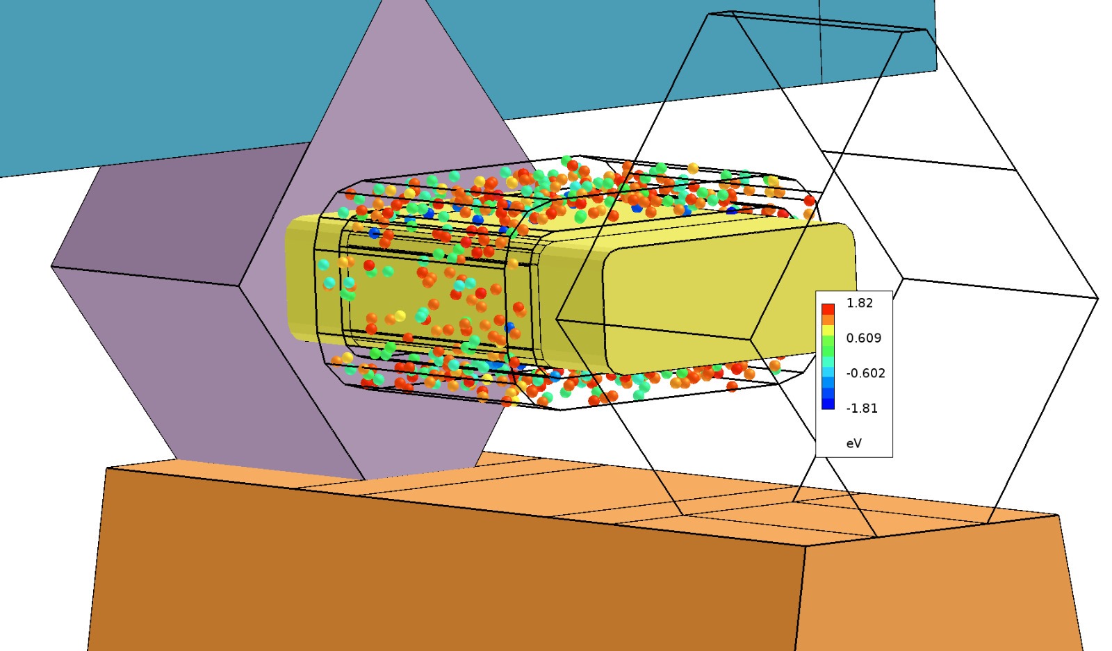
- First, after thoroughly understanding the different future scaling options, the candidate will carry out TCAD simulations of promising emerging architectures (individual devices and whole cells, such as SRAM), with the methodically-identified vulnerable components with realistic defect densities to gain understanding of the aging trends. This step will cover the well-known degradation mechanisms, including Bias Temperature Instability, Hot Carrier Degradation, Time-Dependent Dielectric breakdown, and Self-Heating, for realistic circuit-specific workloads. (These physics-based degradation models have been already implemented in our TCAD software.)
- Furthermore, to simplify and significantly speed up the description of device degradation extracted from the CPU-intensive TCAD above, the candidate will need to calibrate i. Reliability compact models and/or ii. Reliability Machine Learning (ML) models to describe the device aging behavior and trends and to facilitate the next step below. (The compact models are already in place; the ML models are under development in our group. Other degradation mechanisms, such as interconnect Electromigration and Stress Induced Voiding may be also later included as well.)
- In the final step, the candidate should implement novel, large-parameter space optimization techniques find optimal device configurations for given PPAC requirements and specific applications. (Advanced optimization algorithms are already being implemented in our group.)
Required background: A subset of these skills will be beneficial: Semiconductor device physics and TCAD, VLSI reliability fundamentals, basic understanding of VLSI processing, machine learning and optimization essentials, circuit simulation basics
Type of work: 70% modeling/simulation, 20% experimental, 10% literature
Supervisor: Bertrand Parvais
Daily advisor: Ben Kaczer
The reference code for this position is 2025-047. Mention this reference code on your application form.