Novel scalable passivating strategies for perovskite solar modules with minimized upscaling loss
Genk | More than two weeks ago
Developing scalable defect passivation strategies to boost the performance of perovskite solar modules
Energy transition and independence in Europe is more urgent than ever due to the current energy crisis. For a sustainable, secure and competitive energy supply in Europe following the REPowerEU Plan, and for a climate neutral energy supply by 2050, photovoltaics (PV) for electricity generation is seen as a key solution.
In recent years, perovskite solar cells (PSCs) have been under the spotlight as a promising candidate for next-generation PV technology, either in a format of single junction solar cell or in combination with matured silicon PV technology forming a multijunction device. The certified power conversion efficiency (PCE) has reached 26.7% for single junction cells, and 34.6% for perovskite-silicon 2-terminal tandem solar cells. Despite the rapid progress on PCEs, most of the high-performing cells (typically 0.05-0.1 cm2) were fabricated with non-scalable laboratory-scale processes. The performance of large perovskite solar modules to date substantially lags behind those high-performing tiny cells.
To minimize such upscaling losses, uniform deposition of perovskite with high quality over large area substrate is crucial. Defects suppression and passivation in the bulk and at the interfaces are therefore essential for both high initial performance and longer-term stability of perovskite photovoltaics. Commonly, solution processing such as spin coating is widely used for such passivating interlayers at the interfaces between perovskite and charge transport layers. However, such passivating interlayers are often extremely thin (sub-nanometer to a few nanometers), which is rather challenging to have entire coverage with uniformity over large substrate sizes by solution based process. In this regard, there is nowadays a growing interest in exploring industrially compatible deposition methods for such ultrathin passivating interlayers.
This PhD project will focus on in-depth understanding of loss mechanisms during upscaling from tiny cells (typically ~0.1 cm2) to 800 cm2 modules. In the initial stage of this project, a certain perovskite composition (CsxFA1-xPbI3-yBry) will be developed primarily via vapor based approach such as co-evaporation or sequential evaporation, while slot die coating may serve as a backup deposition option. The second objective is the fundamental understanding of the several defects that are present within the developed perovskite layer (in the bulk, at the grain boundaries and surfaces). Based on such understanding, bulk and interface modulation materials will be screened at cell and minimodule level, using scalable deposition methods such as thermal evaporation. The third objective is to successfully integrate the selected passivating strategies in larger (semi-transparent) perovskite modules of 100 and 800 cm2. Figure 1a shows such a ~800 cm2 semi-transparent perovskite module developed at imec. The semi-transparent perovskite module will be applied to perovskite-silicon four-terminal tandem solar modules for high power output (Figure 1b). Indoor and outdoor stability of the selected single junction and tandem modules will be intensively performed. The degradation paths during such ageing tests will be systematically analysed with extensive collaboration with our global partners.
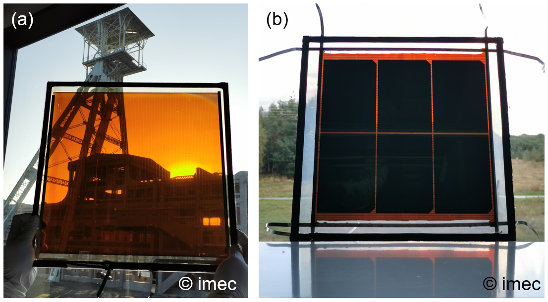
Figure 1 (a) ~800 cm2 semi-transparent perovskite solar module. (b) ~800 cm2 Perovskite-Silicon four-terminal tandem modules, both developed at imec.
The candidate will develop deposition processes for perovskites and defect passivating interlayers, fabricate perovskite solar cells and modules, test their stability under intrinsic stress factors (thermal, light soaking under elevated temperature, etc.) and in real environments. Based on such understanding, mitigation measures for instance via modifying the bulk and the interfaces will be taken to enhance the stability. The candidate will perform advanced characterization on materials and devices (photo- and electro-luminescence, Impedance Spectroscopy, Spectroscopic Ellipsometry, X-ray Photoelectron Spectroscopy (XPS), Ultraviolet Photoelectron Spectroscopy (UPS), Grazing-Incidence Wide-Angle X-ray Scattering (GIWAXS), Scanning Electron Microscopy (SEM), dark and light J-V scans etc.).
The project will be conducted in an interdisciplinary and multicultural team of highly skilled scientists and engineers that work towards commercialization of the next generation of PV technology. The research will be developed in the newly built laboratories at EnergyVille, Genk, working in one of the world’s premier research centers in nanotechnology.
Required background: Materials Science, Materials Engineering, chemistry, semiconductor physics.
Type of work: 70% experimental, 15% modeling, 15% literature
Supervisor: Bart Vermang
Co-supervisor: Jef Poortmans
Daily advisor: Yinghuan Kuang
The reference code for this position is 2025-145. Mention this reference code on your application form.