Extreme Ultraviolet Light Coherent Diffractive Imaging and Scatterometry for Characterization of Nanoscale Semiconductor Structures and Devices
Master projects/internships - Leuven | More than two weeks ago
Enhance the capabilities of extreme ultraviolet nanoscale coherent diffractive imaging and scatterometry with machine learning, advanced reconstruction and data processing algorithms to enable non-destructive imaging and characterization of complex buried semiconductor nanostructures for the next generation’s electronics
As the world around us becomes evermore technologically integrated and devices become smaller, faster, and more efficient, so too do our favorite gadgets become more complex. Inside each one of our devices exists a complicated, multi-dimensional maze of components and materials that ultimately work together to bring us the technological wonders of today. These crucial structures are made via a complex flow of lithographic processes in which layers of material are patterned and deposited, removed and polished, implanted and etched away at the scale of only a few nanometers. The precise manipulation and creation of nanoscale structures is what enables new computing powers, more accurate sensors, and faster microelectronics.
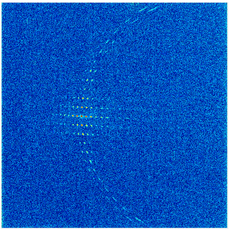
These new technologies only work as long as the underlaying structures are near-perfectly made and the complexity and extreme small size of these components provides significant challenges in their characterization and imaging. Recently, a new imaging and characterization techniques using extreme ultraviolet (EUV) light with a wavelength on a scale of a dozen nanometers have emerged that has the potential to non-destructively image and characterize complex nanostructures both spatially in 3D and compositionally. These techniques, EUV coherent diffractive imaging (CDI) and scatterometry, utilize computer algorithms which process diffraction patterns produced by EUV light reflected from a structure or device to produce an image of the structure with wavelength-scale resolution, or determine various structural parameters with nanometer precision.
CDI is a state-of-the-art computational lensless imaging technique involving registration of diffraction patterns and subsequent numerical reconstruction of samples’ images. While conventional imaging provides only light’s intensity distribution, CDI produces phase information as well. This phase information enables unique imaging capabilities, such as determining the chemical composition, topography, and 3D-imaging of complex, layered materials. When CDI is performed with EUV light, the short wavelength, allows for high-resolution imaging (~10nm) of nanoscale objects, while the transparency of various semiconductor materials, enables non-destructive imaging of buried structures.
Scatterometry is a model-based technique enabling precise characterization of multilayer periodic patterned structures with ~1nm accuracy. It cannot be used for defect inspection as CDI but has higher resolution, sensitivity and speed. In case of a defect present within the beam footprint, scatterometry will yield wider than normal confidence interval indicating presence of anomaly. CDI can then be used on the spot to visualize the defect.
EUV CDI and scatterometry show great promise for non-destructive imaging and characterization of nanostructures; however, we are only beginning to scratch the surface of their power for characterizing actual microelectronic device structures.
Therefore, the aim of the project is development and application of advanced reconstruction and data processing algorithms, including machine-learning-based ones, for the raw experimental diffraction data with the goal of improving quality and resolution of EUV CDI, and precision and accuracy of EUV scatterometry making this project into a crucial step on the road to high-fidelity non-destructive characterization of nanoscale buried structures.
You will mostly be working with algorithms in Python/Matlab, but there also will be an opportunity to work with a unique state-of-the-art EUV laser and vacuum equipment, motorized translation stages and optics, all available at imec’s AttoLab.
Type of Project: Thesis
Master's degree: Master of Science
Master program: Physics
Duration: 9 months
Supervisor: Claudia Fleischmann
For more information or application, please contact the supervising scientist Vitaly Krasnov (Vitaly.Krasnov@imec.be).
Only for self-supporting students.