2019 again was a successful year for imec. What did our 4.000 researchers achieve this year? We highlight a selection of technical innovations, one for every month.
1. Imec continues its journey of logic devices scaling
At the 2019 IEDM Conference, imec has presented the forksheet device as the ultimate solution to push CMOS scaling towards the sub-3nm technology node. The forksheet device can be considered a natural extension of vertically stacked nanosheet devices. Contrary to nanosheet devices, the forksheet architecture allows a much tighter spacing between n- and p-type devices. This results in a 10% performance boost and 20% cell area reduction compared to nanosheet devices – as shown by first standard cell simulations.
Beyond CMOS, imec has confirmed the potential of FETs with 2D-material channels for extreme transistor scaling. At 2019 IEDM, imec researchers showed fabricated devices with MoS2 in their channel, having scaled contact length and channel length as small as 13nm and 30nm respectively. They also identified a path to further improvements aiming at mass production in industrial 300mm fabs.
At technology nodes of 3nm and beyond, routing congestion and a dramatic RC (resistance-capacitance product) delay have become the main challenges for scaling the back-end-of-line structures. At its technology forum ITF USA 2019, imec has presented a dual-damascene 21nm pitch test vehicle that is relevant for manufacturing the 3nm logic technology node. The proposed interconnect technology can be improved by adding scaling boosters, such as buried power rail, SuperVia and fully self-aligned vias. This involves a shift from scaling at logic cell level towards scaling at system level – requiring a STCO (system-technology co-optimization)-oriented approach.
Finally, in a 2019 Nature publication, imec has demonstrated that the steep subthreshold-slope observed in ferroelectric FETs (FeFETs) can be explained by the non-linear positive capacitance of ferroelectric materials. This explanation sheds new light on the sub-60mV/dec behavior of FeFETs, which has often been attributed to the existence of a negative capacitance in ferroelectric capacitors.
2. New milestone for next-generation batteries is good news for e-cars
The end of 2017, imec reached the headlines with a new kind of electrolyte for next-generation batteries. This new kind of batteries could enable the true breakthrough for long-range e-cars. The envisioned roadmap leads towards solid-state batteries with energy densities of 1000Wh/L at 2-3C (by 2024). In 2019, a new milestone was reached in the battery research with a doubling of the energy density (now 400Wh/L) at a charging speed of 0.5C (2 hours) and the setup of a pilot line at the EnergyVille Campus in order to scale up the battery development. Read the different press releases about the battery milestones, from 2017 till now via this link.

Detail of pilot line equipment for battery research
3. More sensing capabilities and user-friendliness for health patch
At the Consumer Electronics Show 2019, imec and TNO showcased a new version of their health patch. Developed in the framework of the Holst Centre in Eindhoven, the new health patch offers increased comfort to the wearer (thanks to the use of skin-friendly and biocompatible materials) and a long battery life (thanks to increased integration). It can also be manufactured at a fraction of the cost of previous generations, making it a user-friendly, disposable solution for ambulant patient monitoring.
Imec spinoff Bloomlife also exploits the unique assets of the chip at the heart of these health patches. At FutureSummits, they showcased a prototype of the world’s first wearable 5-channel electrocardiogram (ECG) chip to continuously and accurately monitor fetal heart rate and mobility, two important indicators of a baby’s wellbeing. With this chip, they have created a wearable ECG system that can accurately measure the fetal ECG as early as week 20 in a woman’s pregnancy.
4. Imec turns radar technology into tool for presence detection, gesture recognition and non-contact vital sign monitoring
At the 2019 International Solid-State Circuits Conference (ISSCC2019), imec described its radar transceiver as an efficient, low-cost solution for presence detection in smart building solutions. The power consumption of the radar is below 1mW, which is 100 times lower than other solutions. It is capable of detecting even micro-movements from human respiration, up to a distance of 15 meters. This performance makes it a breakthrough solution for low-cost battery-powered presence-detection and people counting applications in offices, hospitals and on industrial sites. The new 8GHz UWB radar was developed by imec the Netherlands (within the framework of Holst Centre, Eindhoven).
At FutureSummits, a compact highly-sensitive 140GHz MIMO (multiple-input multiple-output) radar system was presented. Its use for gesture recognition was demonstrated, supporting intuitive man-machine interactions. In addition, the ultra-fine resolution of this radar allows the detection of micro-skin movements related to vital sign monitoring applications like non-contact driver monitoring or patient monitoring.
5. Imec publishes white paper on distance bounding protocol for Bluetooth Low Energy radios
In the future, we will need secure location and proximity information for a variety of applications such as secure access to our home, opening our car without a key, and contactless payment of our groceries. In all these scenarios, wireless technology is used to ensure 'secure proximity' between our 'key' - e.g. a smartphone or smartwatch - and the 'device' we want to access. The white paper provides a solution for using Bluetooth as a wireless technology for secure location and proximity.
6. Whole genome sequencing becomes an affordable reality for patients
On international DNA day (April 25), imec’s ExaScience Life Lab, and its partners in the GAP imec.icon project revealed their Genome Analytics Platform (GAP) platform, a unique platform that can perform a full genome analysis of 48 samples in only 48 hours and at an acceptable cost. The GAP platform enables the widespread clinical use of whole genome sequencing. Since the 1,000-dollar genome is almost a reality, turning the raw sequencing data into ‘knowledge’ and useful information for doctors has become the economic bottleneck. Researchers and industry leaders in the GAP project have now tackled this challenge by developing a new genomic analytics platform that bridges the gap between the low cost of sequencing and the high cost of analyzing raw sequencing data. It enables not only researchers, but also doctors, to analyze and compare genome data for diagnosis, prognosis, or treatment selection. More information about the imec.icon-project can be found here. Read the full press release here.
7. Monolithic integration makes infrared image sensors cheaper and hyperspectral image sensors make the Abbey of Tongerlo more famous
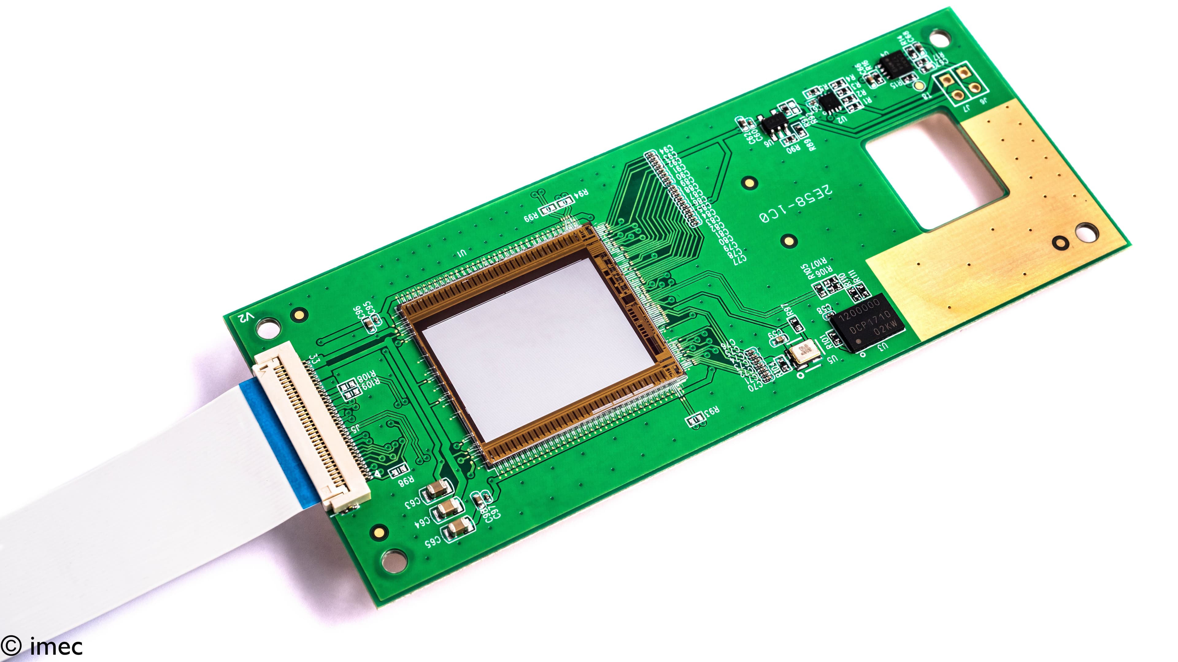
Imec developed a new thin-film monolithic image sensor that captures light in the near-infrared (NIR) and short-wavelength infrared (SWIR). Based on a monolithic approach, the process promises an order of magnitude gain in fabrication throughput and cost compared to processing today’s conventional IR imagers, while at the same time enabling multi-megapixel resolution. IR imagers are used in a wide variety of applications, and imec’s new technology greatly extends their possibilities, including surveillance, biometric identification, virtual reality, machine vision, and industrial automation.
For yet another application, the study of paintings, another imec image sensor came in handy in 2019: the hyperspectral sensor. Hyperspectral cameras divide the light reflected by an object into many narrow spectral bands, which they register and process separately. This way, they capture a spectral signature for each pixel in an image. Imec makes hyperspectral single-chip imagers that can be mass produced and are extremely compact. For many applications, imagers can be built at a price much closer to a normal camera, than to a research instrument, thanks to the technology used to make ordinary computer chips. The cameras designed around these chips are light and compact, making them suitable for a wide range of applications in, for example, precision agriculture or medical instrumentation. The imaging devices themselves can be flexibly designed to meet the demands of the application by selecting the spectral bands and resolution that best suit that application (Read more about it in this article). In 2019, a dedicated hyperspectral camera was used by the team of the American art historian Jean-Pierre Isbouts to study the canvas of ‘The Last Supper’ in the Abbey of Tongerlo. His findings surprised everyone: the painting was probably made in Leonardo da Vinci's studio in Milan, and the head of apostle Johannes was most probably painted by the master himself. Also, In Florida, the hyperspectral camera was used in the fight against pythons, a true plague in the everglades.
8. Imec and its research labs at Ghent University advance Si photonics technology for multiple applications
From the datacenter network down to the chip level, silicon photonics is a prime technology to scale optical interconnects to the desired bandwidth density, power and cost. But silicon photonics can enable applications far beyond datacenter interconnects. Think about biophotonics-on-chip, a relatively new research domain that will be very important for diagnostics, therapy and follow up. With photonic-electronic hybrid chips, one can make revolutionary healthcare solutions with the main characteristic of being compact, smart, low-cost and easy to use. And, integrated optical spectral sensing solutions can benefit an even wider range of applications and markets, including precision agriculture, food analysis or colorimetric applications for industrial and consumer markets.
Imec continued to address the key challenges in developing optical interconnect technology for the next generation of data centers. At the 2019 ECOC conference, imec, together with IDLab and the Photonics Research Group, both imec research labs at Ghent University, demonstrated building blocks that help pave the way for 400Gb/s and beyond optical links as well as for co-packaged optics in next-gen datacenter switches.
In addition, researchers from imec, the Photonics Research Group and MIT have provided a crucial step in realizing quantum optical circuits – circuits that connect large numbers of photonics devices. They have used 2D materials to fabricate an on-chip single photon emitter – central building block of such an integrated quantum circuit. The 2D-based single photon emitters were then coupled to a CMOS-compatible silicon nitride waveguide. The results, published in Nature Communications, pave the way for scaling up quantum photonic devices.
With the advent of large-scale quantum computers, novel encryption techniques are required that are secure against quantum-based threats. In 2019, imec and National University of Singapore (NUS) entered into a five-year collaboration agreement for developing scalable and cost-effective quantum cryptographic systems. They will jointly develop quantum key distribution (QKD) and quantum random number generation (QRNG) – two essential building blocks for enabling quantum cryptography. In a later stage, they will work on a compact, fully integrated photonic quantum transmitter prototype chip.
Roel Baets, full professor at Ghent University, has been named the 2020 John Tyndall Award recipient. Roel Baets, who leads the Photonics Research Group, is recognized for “seminal research in silicon photonics and for driving the foundry model in this field”. The John Tyndall Award, jointly sponsored by the IEEE Photonics Society and the Optical Society (OSA), is presented annually to a single individual who has made outstanding contributions in any area of optical-fiber technology. Congratulations to Roel Baets!
9. Imec monolithically co-integrates GaN half-bridge and drivers in a single GaN-IC chip
Today, gallium-nitride (GaN) power components such as half-bridges are typically fabricated as separate components, either in individual packages or integrated in one package. Realizing these half-bridges on chip would however bring many benefits – in terms of complexity, cost and performance of power electronics. The monolithic integration of these components on chip by using GaN-on-Si technology is however very challenging. Building on its GaN-on-SOI and GaN-on-QST® technology platforms, imec has demonstrated a functional GaN half-bridge monolithically integrated with drivers in one GaN-IC chip. The solution paves the way to boosting GaN performance and enabling true GaN-IC technology. More info in the press release.
10. Imec shrinks Raman spectroscope onto a chip
At SPIE BIOS and SPIE Photonics West 2019, imec presented an on-chip solution for Raman spectroscopy, based on a newly patented concept. It provides high optical throughput and high spectral resolution. The solution could pave the way for affordable high-end handheld Raman spectroscopy devices opening up many new applications. More details can be found in this article.

Imec’s On-chip RAMAN spectroscopy solution
11. Imec, TNO and Cartamundi create smart labels to allow paper and plastic objects to communicate with touchscreens.
Imec, TNO and Cartamundi developed a flexible capacitive identification tag, a so-called C-touch tag, which communicates with standard touchscreens such as the screen of your smartphone. The tags are very thin and pliable and can be integrated in a wide range of paper or plastic objects (e.g. tickets, certified documents, payment cards, ...). By placing these objects on a touchscreen, a connection can be made to the internet. You could use the technology in entrance tickets (because it is more difficult to copy and therefore safer), or for payments (put your bank card against your computer screen to make a payment), or in pawns and dice in combination with a screen-game board. The results, developed as part of the Holst Centre, an open innovation initiative of imec and TNO, were published in December 2019 in Nature Electronics. More details can be found in this press release.
12. Imec team in the finals of DARPA Spectrum Collaboration Challenge to develop the best possible wireless network system
As the only European team, IDLab (an imec research group at the university of Antwerp and Ghent,) together with scientist form Rutgers University (US) participated in the DARPA challenge. The prestigious DARPA challenges are global competitions in which teams of researchers work around a specific theme to overcome a problem that affects the entire world. One challenge at the end of the 1960s, for example, was to connect computers with each other. This produced the ARPANET, the predecessor of the Internet as we know it today. More recently, the DARPA Grand Challenge also sparked the idea for Google’s self-driving car.
In 2017, a new DARPA Challenge was launched, challenging scientists to develop the best possible wireless network system – one which also works reliably in e.g. crisis conditions. IDLab decided to focus their solution on artificial intelligence. Things can go wrong nowadays if the digital information sent out by different wireless devices ‘collides’ because the devices are using the same channel on the wireless spectrum. By teaching wireless devices like smartphones to figure out what other devices are doing and predict when they will use which channels, one can avoid these collisions. That way, it’s no longer necessary to make wireless communication plans or agreements in advance – something that’s impossible in crisis situations anyway.
The interdisciplinary group of researchers eventually became 6th in the challenge and predict that such artificial intelligence-based solutions could be ready for use in the short term. They are working with Antwerp’s fire department, for example to enable them to stream live images of fires to their command vehicles. And to get those images from the fire site to the command vehicle, we need to build a new wireless network. The team became 6th in the final of the DARPA challenge on October 23.
Published on:
1 January 2020


